
 My Inquiry
 My Account


Analog Devices Inc. HMC822LP6CE
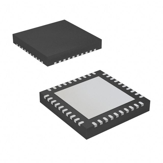
- Part No.:
- HMC822LP6CE
- Manufacturer:
- Analog Devices Inc.
- Package:
- 40-VFQFN Exposed Pad
- Datasheet:
-
 HMC822LP6CE.pdf
- Description:
- IC PLL W/VCO FRACTIONAL-N 40-QFN
- Quantity:
- Payment:

- Shipping:

Inventory:1,191
Please send an inquiry. Send us your inquiry, and we will respond immediately.
Product details
Overview
HMC822LP6CE from Analog Devices (formerly Hittite Microwave) is a fully integrated Fractional-N Phase-Locked Loop with on-die VCO, operating across three RF bands: 665–825 MHz (÷2), 1330–1650 MHz (fundamental), and 2660–3300 MHz (×2). It delivers ultra-low phase noise (−105 dBc/Hz in-band typ.), <180 fs RMS jitter, and 24-bit frequency resolution (3 Hz typ. step size), serving as a high-performance clock synthesis and local oscillator solution in cellular infrastructure and test equipment.
For engineers reviewing the HMC822LP6CE datasheet, HMC822LP6CE pinout, HMC822LP6CE application, or HMC822LP6CE equivalent, this page provides verified technical context, tri-band output behavior, fractional-N architecture details, real-world power supply requirements, and validated alternative options for RF synthesizer design.
Technical Context
The HMC822LP6CE integrates a tri-band VCO with autocalibration, a low-noise digital phase detector featuring cycle-slip prevention (CSP), a precision charge pump (0.02–2.54 mA), and a 24-bit fractional-N divider with advanced delta-sigma modulation. Its architecture enables ultra-fine frequency resolution while suppressing spurious content and enabling fast frequency hopping.
It supports three output modes-÷2, fundamental, and ×2-each with distinct RF output power levels (e.g., +9 to +13 dBm at fVCO/2, +2.5 to +10.5 dBm at fVCO) and harmonic suppression (e.g., −22 dBc 2nd harmonic in doubler mode). The device requires separate 5 V analog (VPPCP/VDDCP/VCC1/VCC2) and 3.3 V analog/digital (AVDD/DVDD3V/RVDD/etc.) supplies, with thermal resistance of 9 °C/W to ground paddle.
Key Specifications
| Parameter | Value and Actual Design Meaning |
|---|---|
| RF Output Bands | 665–825 MHz (÷2), 1330–1650 MHz (fundamental), 2660–3300 MHz (×2) - enables single-device coverage of LTE/5G FR1 & FR2 bands |
| Phase Noise (in-band) | −105 dBc/Hz typ. - enables wide loop bandwidths (>100 kHz) for fast settling without degrading spectral purity |
| Frequency Resolution | 3 Hz typ. (24-bit fractional divider) - supports precise channel spacing in narrowband comms and radar |
| RMS Jitter | <180 fs - meets stringent timing requirements for high-speed serial links and ADC/DAC sampling clocks |
| Figure of Merit (FOM) | −227 dBc/Hz (fractional mode) - benchmark metric confirming state-of-the-art noise efficiency for its frequency range |
| Charge Pump Range | 0.02–2.54 mA - allows flexible loop filter design across wide PFD frequencies (0.1–125 MHz) |
| Supply Voltages | +5 V (VPPCP/VDDCP/VCC1/VCC2) and +3.3 V (AVDD/DVDD3V/RVDD/VCCHF/VCCPS/VCCPD) - mandates dual-rail PCB layout with strict decoupling |
Pinout & Package
40-lead 6×6 mm QFN package (RoHS-compliant, MSL1, exposed ground paddle); thermal resistance 9 °C/W junction-to-paddle. All ground leads and paddle must be soldered to PCB RF ground per Hittite Application Note.
| Pin/Terminal | Circuit Role | Design Meaning |
|---|---|---|
| 1, 10, 16, 25, 27, 35–36, 39, 40 | Power Supply Inputs | Dedicated rails: AVDD (analog), RVDD (reference), DVDD3V (digital), VPPCP/VDDCP (charge pump), VCC1/VCC2 (VCO), VCCHF/VCCPS/VCCPD (high-frequency analog), BIAS (precision bias reference) |
| 4, 23 | Analog Outputs | CP (charge pump current output) and VTUNE (VCO tuning voltage input) - sensitive nodes requiring guard traces and low-noise filtering |
| 28–29 | RF Differential Outputs | RF_P / RF_N - support ÷2/fundamental/×2 modes; must be shorted externally in doubler mode per datasheet note |
| 15, 30–33 | Digital Control Interface | XREFP (crystal input), CEN (chip enable), SEN/SDI/SCK/LD_SDO (4-wire SPI with lock detect or GPO function) |
| 2, 5–6, 8–9, 11–14, 18–22, 24, 26, 34, 37–38 | No-connect (N/C) | Internally unconnected; externally grounded per measurement conditions - required for RF stability and EMI control |
Key Features
| Feature | Design Value |
|---|---|
| Tri-band VCO with autocalibration | Enables seamless operation across 665–825 / 1330–1650 / 2660–3300 MHz without external tuning components or manual calibration |
| Cycle-slip prevention (CSP) in PD | Reduces frequency hop settling time by preventing phase detector miscounts during large frequency transitions |
| Built-in digital self-test | Allows in-system verification of PLL lock, VCO functionality, and register integrity without external test equipment |
| Exact Frequency Mode | Eliminates fractional spur accumulation over time by dynamically adjusting N-divider to maintain exact target frequency |
| Ultra-low in-band phase noise | −105 dBc/Hz typ. enables wider loop bandwidths (up to ~100 kHz) for faster frequency agility while preserving spectral purity |
Applications
| Cellular Infrastructure | Communications Test Equipment |
|---|---|
|
Use Scenario: Generating local oscillator signals for macrocell and small-cell transceivers supporting LTE and 5G NR in FR1 (sub-6 GHz). IC Role / Device Role / Timing Role: Integrated PLL+VCO providing clean, agile LO synthesis with sub-100 fs jitter for I/Q modulator/demodulator clocking. Use Value: Eliminates discrete VCO + PLL board space; tri-band coverage reduces need for multiple synthesizers across band classes. |
Use Scenario: High-resolution signal generation and analysis in vector signal analyzers and arbitrary waveform generators. IC Role / Device Role / Timing Role: Low-phase-noise frequency source enabling accurate EVM and ACLR measurements at multi-GHz carriers. Use Value: −227 dBc/Hz FOM and <180 fs jitter meet metrology-grade spectral purity requirements for 5G NR conformance testing. |
| Repeaters & Femtocells | Phased Array Systems |
|
Use Scenario: Compact, low-power frequency translation in indoor/outdoor repeaters and residential femtocells. IC Role / Device Role / Timing Role: Single-chip synthesizer delivering stable LOs for up/down-conversion with minimal external components. Use Value: 40-lead 6×6 mm QFN package and integrated VCO reduce BOM count and PCB area vs. discrete solutions. |
Use Scenario: Beamforming element clocking in active electronically scanned arrays (AESA) for radar and satellite communications. IC Role / Device Role / Timing Role: Synchronized multi-channel LO source with deterministic phase relationship across distributed nodes. Use Value: Exact Frequency Mode and CSP ensure repeatable, glitch-free frequency switching critical for coherent beam steering. |
Equivalent & Alternatives
The following parts are listed as comparable options for similar fractional-N PLL with integrated VCO applications.
| Alternative Part | Technical Difference | Application Difference | Selection Advice |
|---|---|---|---|
| HMC830LP6GE | Wider frequency range (31.25–4000 MHz), higher max PFD frequency (250 MHz), but larger 40-lead 7×7 mm package and no built-in self-test | Better suited for wideband test instrumentation requiring >2 GHz coverage; less optimal for space-constrained femtocell designs | Select HMC830LP6GE when broader frequency sweep or higher PFD rate is required; verify PCB land pattern compatibility due to larger footprint |
| ADF4371BCPZ | Higher integration (integrated LDOs, SPI interface with readback), lower typical phase noise (−111 dBc/Hz in-band), but requires external loop filter and has different power sequencing | Preferred for new designs prioritizing ease of use and system-level integration; not drop-in compatible due to different pinout and supply architecture | Choose ADF4371BCPZ for simplified power design and enhanced diagnostics; redesign power delivery and SPI routing versus HMC822LP6CE |
Compared with HMC822LP6CE, HMC830LP6GE offers extended frequency agility at the cost of board area, while ADF4371BCPZ trades pin compatibility for integrated regulation and superior in-band phase noise - both require layout and firmware adaptation.
Availability
HMC822LP6CE is available at Aetrix Electronics and suitable for cellular infrastructure, communications test equipment, and phased array systems requiring stable component supply, long-term lifecycle support, and RoHS-compliant packaging.
Supply support for HMC822LP6CE includes scheduled delivery planning, volume procurement assistance, BOM continuity management, traceable sourcing, and lifecycle availability coordination for OEM customers, industrial embedded developers, connected-device designers, and electronics production programs.
Manufacturer
Analog Devices acquired Hittite Microwave in 2014 and maintains its high-frequency RF product lines with emphasis on performance-critical wireless infrastructure and defense applications.
The HMC822LP6CE belongs to the Hittite PLLs with Integrated VCOs family, designed specifically for compact, low-phase-noise frequency synthesis in multi-band wireless base stations and instrumentation where board space and spectral purity are constrained.
FAQ
What output frequency bands does the HMC822LP6CE support?
The HMC822LP6CE supports three distinct RF output bands: 665–825 MHz (via internal ÷2), 1330–1650 MHz (fundamental VCO output), and 2660–3300 MHz (via internal ×2 doubler). Each band has specified output power and harmonic suppression - for example, +9 to +13 dBm at fVCO/2 and −22 dBc 2nd harmonic in doubler mode. Band selection is controlled via register configuration and external RF path routing.
Does the HMC822LP6CE require external loop filter components?
Yes, the HMC822LP6CE requires an external passive loop filter between the charge pump (CP pin) and VTUNE (VCO tuning input). The filter topology and component values depend on desired loop bandwidth, phase margin, and reference frequency - Hittite's application note recommends contacting the factory for optimized values. No internal loop filter is integrated.
What is the significance of "Exact Frequency Mode" in the HMC822LP6CE?
Exact Frequency Mode dynamically adjusts the fractional-N divider ratio to eliminate long-term frequency error accumulation caused by rounding in standard fractional division. For the HMC822LP6CE, this ensures the output remains precisely locked to the target frequency over time - critical for applications like DDS replacement and high-accuracy signal generation where drift must be minimized.
How is the HMC822LP6CE powered, and what are the key supply requirements?
The HMC822LP6CE requires two independent supply domains: +5 V for analog charge pump and VCO core/buffers (VPPCP, VDDCP, VCC1, VCC2), and +3.3 V for digital, reference, and high-frequency analog sections (DVDD3V, RVDD, AVDD, VCCHF, VCCPS, VCCPD). Each rail has tight tolerance specs (±4% for 5 V, ±6% for 3.3 V) and dedicated decoupling - improper sequencing or insufficient filtering causes instability or degraded phase noise.
Can the HMC822LP6CE operate in all three RF bands simultaneously?
No, the HMC822LP6CE operates in only one RF band at a time - ÷2, fundamental, or ×2 - selected via register configuration and external RF path setup. Simultaneous multi-band output is not supported. However, fast reconfiguration (<100 µs typical lock time) allows rapid band switching in time-division systems such as TDD radios or multi-standard test equipment.
HMC822LP6CE Specifications
- Product attributes
- Attribute value
- Manufacturer:
- Analog Devices Inc.
- Series:
- -
- Package/Case:
- 40-VFQFN Exposed Pad
- Packaging:
- Bulk
- Product Status:
- Obsolete
- Programmable:
- Not Verified
- Type:
- -
- PLL:
- Yes
- Input:
- Clock
- Output:
- Clock
- Number of Circuits:
- 1
- Ratio - Input:Output:
- 1:1
- Differential - Input:Output:
- No/Yes
- Frequency - Max:
- 3.3GHz
- Divider/Multiplier:
- Yes/Yes
- Voltage - Supply:
- 3V ~ 5.2V
- Operating Temperature:
- -40°C ~ 85°C
- Mounting Type:
- Surface Mount
- Grade:
- -
- Qualification:
- -
- Supplier Device Package:
- 40-QFN (6x6)
HMC822LP6CE FAQ
1.How can I place an order for HMC822LP6CE through Aetrix?
Please submit a Request for Quotation (RFQ) for HMC822LP6CE on Aetrix. Our sales agent will provide a competitive quotation and guide you through the order confirmation once you accept the terms.
2.Are the price and stock information for HMC822LP6CE reliable?
The price and inventory of HMC822LP6CE are updated periodically and may fluctuate due to market conditions. Stock and pricing data are typically refreshed every 24 hours. Quotation validity for HMC822LP6CE is usually 5 days.
3.What payment methods are accepted for HMC822LP6CE?
We accept Wire Transfer, PayPal, Credit Card, Western Union, MoneyGram, and Escrow for HMC822LP6CE transactions.
Note: Certain payment methods may incur a processing fee.
4.How is shipping managed for HMC822LP6CE?
HMC822LP6CE orders can be shipped via leading logistics carriers, including DHL, UPS, FedEx, TNT, or Registered Mail.
Once your HMC822LP6CE order is processed, you will receive an email with the shipment details and tracking number.
Note: Tracking information may take up to 24 hours to appear. Express delivery typically takes 3–5 business days.
5.How can I obtain technical support or documentation for HMC822LP6CE?
For technical support, including HMC822LP6CE datasheets, pinout diagrams, or application guidance, please contact our engineering support team. They can provide detailed documentation and assistance for your HMC822LP6CE requirements.
6.How does Aetrix verify that HMC822LP6CE is sourced from the original manufacturer or authorized distributors?
All HMC822LP6CE products on Aetrix are procured from qualified distributors and authorized channels. Our dedicated quality assurance team conducts strict verification, including traceability checks and, if necessary, third-party testing. This ensures that HMC822LP6CE meets industry standards.
7.What is the process for return or replacement of HMC822LP6CE?
All HMC822LP6CE units undergo pre-shipment inspection (PSI). If there is an issue with HMC822LP6CE, returns or replacements are accepted under the following conditions:
1.Quantity discrepancies, incorrect items, or visible external defects (such as breakage or corrosion), acknowledged by Aetrix.
2.The issue is reported within 90 days of delivery.
3.The HMC822LP6CE part is unused and in its original packaging.
Return procedure for HMC822LP6CE:
1.Submit a request within 90 days.
2.Obtain a Return Material Authorization (RMA) from Aetrix.
HMC822LP6CE Tags

-
CD74HCT4046AM96
Texas Instruments

-
MC14046BDWR2G
onsemi

-
501MILFT
Renesas
-
CD74HC7046AM
Texas Instruments

-
CDCVF2505PWR
Texas Instruments

-
RC19004A100GNL#KB0
Renesas

-
SI5351A-B-GTR
Skyworks Solutions Inc.

-
CY2305SXI-1T
Infineon Technologies
-
570BILFT
Renesas

-
CDCE913PWR
Texas Instruments
-
CY2305SXI-1HT
Infineon Technologies

-
DS1086LU+T
Analog Devices Inc./Maxim Integrated
Tech Hub

A practical engineering guide to 3.3V and 5V logic compatibility, input thresholds, resistor dividers, translator ICs, MOSFET level shifting, I2C pull-ups, timing limits and power-sequencing risks.

The 74HC595 uses push-pull logic outputs, while the TPIC6B595 uses 50 V open-drain DMOS sinks for higher-power loads. This guide compares timing, current limits, 3.3 V interfacing, load wiring, thermal…

The 74HC595 converts serial data into eight stable parallel outputs. This guide covers pin functions, shift and storage timing, OE and MR behavior, drive-current limits, cascading, voltage compatibilit…

A technical comparison of level-sensitive latches and edge-triggered flip-flops, covering timing windows, setup and hold limits, master–slave operation, time borrowing, race-through, HDL inference and…

A D latch stores one bit while Enable controls when data can pass. This reference covers gate-level operation, truth tables, transparency, setup and hold timing, LE versus OE, common ICs and practical …

An SR latch stores one bit through cross-coupled feedback. This engineering reference covers NOR and NAND implementations, truth tables, forbidden-state recovery, gated operation, switch debouncing, fa…

Latch circuits retain one bit through feedback. This technical reference covers SR and D latches, truth tables, transparency, timing limits, latch-versus-flip-flop behavior, applications and common log…

An engineering guide to LED driver operation, constant-current and constant-voltage outputs, linear and switching topologies, dimming, IC selection, calculations, replacement compatibility, and fault c…

Operational amplifier guide covering op amp basics, feedback, ideal vs real op amps, common configurations, buffer circuits, offset, bias current, gain-bandwidth, slew rate, rail-to-rail limits and sel…

Jumper cables guide covering safe connection order, red and black clamp placement, final ground connection, cable gauge, length, clamp quality, copper vs CCA cables, jump starter comparison and battery…


