
 My Inquiry
 My Account


Analog Devices Inc. HMC870LC5
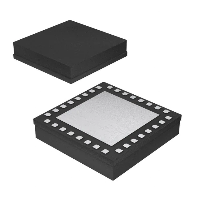
- Part No.:
- HMC870LC5
- Manufacturer:
- Analog Devices Inc.
- Category:
- RF Modulators
- Package:
- 32-TFQFN Exposed Pad
- Datasheet:
-
 HMC870LC5.pdf
- Description:
- RF MODULATOR 0HZ-20GHZ 32TFQFN
- Quantity:
- Payment:

- Shipping:

Inventory:2,811
Please send an inquiry. Send us your inquiry, and we will respond immediately.
Product details
Overview
HMC870LC5 from Analog Devices (formerly Hittite Microwave) is a GaAs MMIC pHEMT distributed driver amplifier optimized for MZ optical modulator biasing in high-speed fiber-optic transmission systems. It delivers 17 dB gain, 8 Vp-p saturated output swing, and <300 fs additive RMS jitter at 10 Gbps - enabling precise drive of low-Vπ modulators in metro/long-haul DWDM infrastructure.
For engineers reviewing the HMC870LC5 datasheet, HMC870LC5 pinout, HMC870LC5 application, or HMC870LC5 equivalent, key selection criteria include its DC–20 GHz bandwidth, adjustable cross-point and output amplitude (2.5–8 Vp-p), wide 3.3–7 V supply range, and 32-lead 5×5 mm SMT package with internal 50 Ω RF matching.
Technical Context
The HMC870LC5 employs a distributed amplifier architecture using GaAs pHEMT devices to achieve flat gain (±0.5 dB) from DC to 20 GHz while maintaining low group delay variation (±15 ps over 1–12 GHz). Its RF I/Os are internally matched to 50 Ω, eliminating external matching networks for broadband operation.
It features three independent bias controls: Vgg adjusts gate voltage (−2 V to 0 V) to set drain current (140–165 mA), Vctl (0–2 V) scales output swing amplitude, and Vdd (3.3–7 V) directly determines maximum output voltage and power dissipation (<0.4 W at 3.6 Vp-p, <1 W at 8.5 Vp-p).
Key Specifications
| Parameter | Value and Actual Design Meaning |
|---|---|
| Frequency Range | DC to 20 GHz - supports NRZ/RZ modulation up to 40 Gbps DQPSK without external equalization. |
| Small Signal Gain | 17.5 dB typ. (1–8 GHz) - provides sufficient headroom for cascaded modulator stages with margin. |
| Saturated Output Swing | 8 Vp-p - drives low-Vπ lithium niobate or silicon photonics MZ modulators requiring >6 Vp-p. |
| Additive RMS Jitter | 300 fs @ 10 Gbps - meets stringent jitter budget for 10G/40G coherent and PAM4 optical links. |
| Supply Voltage Range | +3.3 V to +7 V - enables scalable power/performance trade-off: 0.33 W at 3.3 V, 1.115 W at 7 V. |
| Input/Output Impedance | 50 Ω internally matched - eliminates discrete matching components and simplifies PCB layout. |
| Rise/Fall Time | 20 ps (20%–80%) - preserves signal integrity for 22.5 Gbps NRZ eye opening. |
Pinout & Package
Package: 32-lead, 5 mm × 5 mm leadless surface-mount ceramic package (alumina body, gold-over-nickel plating), MSL3, thermal resistance 59.4 °C/W (channel-to-ground paddle).
| Pin/Terminal | Circuit Role | Design Meaning |
|---|---|---|
| 2 | Vctl | Output swing amplitude control (0–2 V); sets nominal 8 Vp-p at +1 V. |
| 5 | RFIN | DC-coupled 50 Ω RF input; requires AC coupling per recommended operation. |
| 6, 20 | GND | RF/DC ground; must be soldered to PCB ground plane with multiple vias. |
| 13 | Vgg | Gate bias control (−2 V to 0 V); adjusts Idd from 100 mA to 165 mA. |
| 15, 16, 29, 30 | ACGx | Low-frequency termination points; require external bypass capacitors per application circuit. |
| 21 | RFOUT & Vdd | Combined RF output and drain supply node; DC bias applied via broadband bias tee or network. |
| 1, 3, 4, 7–12, 14, 17–19, 22–28, 31, 32 | N/C | No internal connection; must be externally grounded for RF stability and thermal conduction. |
Key Features
| Feature | Design Value |
|---|---|
| Cross-point adjustment | Vgg tuning enables fine control of eye crossing percentage (e.g., 50% ±5%) without external feedback. |
| Scalable power dissipation | Power scales linearly with Vdd: 0.33 W @ 3.3 V, 0.70 W @ 5 V, 1.115 W @ 7 V - supports thermal-aware system design. |
| Wideband 50 Ω matching | Eliminates external matching components across DC–20 GHz, reducing BOM count and layout sensitivity. |
| Low-temp-coefficient gain | Gain drift ≤0.045 dB/°C (10–20 GHz) - maintains consistent modulation depth across −40°C to +85°C operating range. |
| ESD robustness | Class 1A HBM rating - survives handling per JEDEC JS-001 without special precautions beyond standard ESD protocols. |
Applications
| 10 Gbps NRZ MZ Modulator Driver | 40 Gbps DQPSK Transmission |
|---|---|
Use Scenario: Driving low-Vπ lithium niobate Mach-Zehnder modulators in 10G Ethernet or OTU2 line cards. IC Role / Device Role / Timing Role: High-fidelity voltage-mode driver providing precise differential swing and minimal jitter to maintain extinction ratio and BER. Use Value: 300 fs additive jitter and ±0.5 dB gain flatness ensure >30 dB ER and <10−12 BER at 10.7 Gbps without forward error correction. |
Use Scenario: Dual-channel drive for IQ-modulated 40G DQPSK transmitters in coherent metro networks. IC Role / Device Role / Timing Role: Split-path broadband driver delivering matched amplitude/phase response to two parallel MZ arms. Use Value: 20 ps rise/fall time and <15 ps group delay variation preserve constellation fidelity across I/Q paths at 22.5 Gbaud symbol rate. |
| Broadband Test Equipment Gain Block | Military & Space Optical Links |
Use Scenario: Wideband amplification stage in vector network analyzers or high-speed bit-error-rate testers. IC Role / Device Role / Timing Role: Flat-gain, low-jitter active component extending frequency coverage to 20 GHz without calibration drift. Use Value: 17 dB gain with ±0.5 dB flatness and 20 GHz 3-dB bandwidth enable accurate S-parameter measurement up to K-band. |
Use Scenario: Radiation-tolerant optical transmitter in satellite interconnect or airborne avionics data links. IC Role / Device Role / Timing Role: High-reliability modulator driver operating across −40°C to +85°C with no derating below 85°C ambient. Use Value: 175°C channel temperature rating and Class 1A ESD support extended mission life in uncontrolled thermal environments. |
Equivalent & Alternatives
The following parts are listed as comparable options for similar optical modulator driver applications.
| Alternative Part | Technical Difference | Application Difference | Selection Advice |
|---|---|---|---|
| HMC1099LP5E | Higher 25 GHz bandwidth, 22 dB gain, but fixed 5 V supply and no Vctl adjustment; 32-lead 5×5 mm package. | Optimized for 100G PAM4 where wider bandwidth outweighs amplitude flexibility. | Select HMC1099LP5E when >22 GHz small-signal BW is required and output swing is fixed by system design. |
| LMH5401IRHAT | Si-based, 18 GHz BW, 16 dB gain, 6.5 Vp-p max, integrated DC restoration, but higher 550 fs jitter and narrower temp range (−40°C to +85°C). | Cost-sensitive commercial 10G LR/ER modules where GaAs performance is not mandatory. | Select LMH5401IRHAT for lower-cost, non-military designs accepting higher jitter and reduced output swing. |
Compared with HMC1099LP5E and LMH5401IRHAT, the HMC870LC5 uniquely balances ultra-low jitter (300 fs), wide supply scalability (3.3–7 V), and analog cross-point control - making it optimal for precision-driven 10G/40G metro systems requiring field-adjustable drive conditions.
Availability
HMC870LC5 is available at Aetrix Electronics and suitable for 10G/40G optical transceivers, test equipment front-ends, and military-grade photonic subsystems requiring stable component supply across extended temperature and lifecycle requirements.
Supply support for HMC870LC5 includes scheduled delivery planning, volume procurement assistance, BOM continuity management, traceable sourcing, and lifecycle availability coordination for OEM customers, industrial embedded developers, connected-device designers, and electronics production programs.
Manufacturer
Analog Devices acquired Hittite Microwave in 2014 and integrates its high-frequency RF/microwave portfolio into precision analog and RF solutions for communications, defense, and instrumentation.
The HMC870LC5 belongs to Hittite's optical modulator driver product line, designed specifically for high-fidelity, low-jitter drive of MZ interferometers in metro and long-haul fiber-optic infrastructure.
FAQ
What is the maximum output voltage swing of the HMC870LC5?
The HMC870LC5 delivers up to 8 Vp-p saturated output swing when operated at Vdd = +7 V and Vctl = +1 V. Output amplitude is continuously adjustable from 2.5 Vp-p to 8 Vp-p via the Vctl pin (0–2 V), enabling precise matching to modulator Vπ requirements without external attenuators or amplifiers. This capability is confirmed across all specified supply voltages (3.3 V to 7 V) and data rates up to 22.5 Gbps.
Does the HMC870LC5 require external impedance matching?
No, the HMC870LC5 has RF input and output ports internally matched to 50 Ω across DC to 20 GHz. The RFIN pin is DC-coupled and requires only AC coupling per recommended operation, while RFOUT is combined with the Vdd supply node and must be biased through a broadband bias tee or external network. No external matching components are needed for nominal 50 Ω system integration.
How is cross-point adjustment implemented on the HMC870LC5?
Cross-point adjustment on the HMC870LC5 is achieved by tuning the Vgg pin (gate bias voltage) between −1 V and 0 V. This varies the amplifier's quiescent point to shift the eye diagram crossing percentage - typically targeting 50% ±5% - without requiring external feedback loops or digital control. The effect is verified in eye diagrams at 11.25 Gbps and 22.5 Gbps under multiple Vdd conditions.
What is the thermal management requirement for continuous operation of the HMC870LC5?
The HMC870LC5 has a channel-to-ground thermal resistance of 59.4 °C/W and a maximum channel temperature of 175 °C. At full power (Vdd = +7 V, Idd = 165 mA → 1.115 W), junction temperature rise is ~66 °C above board temperature. To stay within the −40°C to +85°C case operating range, the PCB ground paddle must be soldered to a solid ground plane with ≥8 thermal vias, and forced-air cooling or heatsinking is recommended for sustained >1 W dissipation.
Is the HMC870LC5 compatible with both NRZ and RZ modulation formats?
Yes, the HMC870LC5 is explicitly validated for both 10 Gbps NRZ and RZ transmission, as well as 40 Gbps DQPSK. Eye diagrams confirm clean 11.25 Gbps RZ and 22.5 Gbps NRZ operation with RMS jitter ≤2.422 ps and rise/fall times ≤22 ps. Its flat group delay (±15 ps) and gain response preserve pulse shape integrity critical for RZ duty-cycle fidelity and NRZ edge timing.
HMC870LC5 Specifications
- Product attributes
- Attribute value
- Manufacturer:
- Analog Devices Inc.
- Series:
- -
- Package/Case:
- 32-TFQFN Exposed Pad
- Packaging:
- Strip
- Product Status:
- Active
- Function:
- Modulator Driver
- LO Frequency:
- -
- RF Frequency:
- 0Hz ~ 20GHz
- P1dB:
- -
- Noise Floor:
- -
- Output Power:
- -
- Current - Supply:
- -
- Voltage - Supply:
- 7V
- Test Frequency:
- -
- Mounting Type:
- Surface Mount
- Supplier Device Package:
- 32-QFN (5x5)
HMC870LC5 FAQ
1.How can I place an order for HMC870LC5 through Aetrix?
Please submit a Request for Quotation (RFQ) for HMC870LC5 on Aetrix. Our sales agent will provide a competitive quotation and guide you through the order confirmation once you accept the terms.
2.Are the price and stock information for HMC870LC5 reliable?
The price and inventory of HMC870LC5 are updated periodically and may fluctuate due to market conditions. Stock and pricing data are typically refreshed every 24 hours. Quotation validity for HMC870LC5 is usually 5 days.
3.What payment methods are accepted for HMC870LC5?
We accept Wire Transfer, PayPal, Credit Card, Western Union, MoneyGram, and Escrow for HMC870LC5 transactions.
Note: Certain payment methods may incur a processing fee.
4.How is shipping managed for HMC870LC5?
HMC870LC5 orders can be shipped via leading logistics carriers, including DHL, UPS, FedEx, TNT, or Registered Mail.
Once your HMC870LC5 order is processed, you will receive an email with the shipment details and tracking number.
Note: Tracking information may take up to 24 hours to appear. Express delivery typically takes 3–5 business days.
5.How can I obtain technical support or documentation for HMC870LC5?
For technical support, including HMC870LC5 datasheets, pinout diagrams, or application guidance, please contact our engineering support team. They can provide detailed documentation and assistance for your HMC870LC5 requirements.
6.How does Aetrix verify that HMC870LC5 is sourced from the original manufacturer or authorized distributors?
All HMC870LC5 products on Aetrix are procured from qualified distributors and authorized channels. Our dedicated quality assurance team conducts strict verification, including traceability checks and, if necessary, third-party testing. This ensures that HMC870LC5 meets industry standards.
7.What is the process for return or replacement of HMC870LC5?
All HMC870LC5 units undergo pre-shipment inspection (PSI). If there is an issue with HMC870LC5, returns or replacements are accepted under the following conditions:
1.Quantity discrepancies, incorrect items, or visible external defects (such as breakage or corrosion), acknowledged by Aetrix.
2.The issue is reported within 90 days of delivery.
3.The HMC870LC5 part is unused and in its original packaging.
Return procedure for HMC870LC5:
1.Submit a request within 90 days.
2.Obtain a Return Material Authorization (RMA) from Aetrix.
HMC870LC5 Tags
-
LTC5599IUF#TRPBF
Analog Devices Inc.
-
LTC5599IUF#PBF
Analog Devices Inc.
-
LTC5589IUF#PBF
Analog Devices Inc.
-
ADL5375-05ACPZ-R7
Analog Devices Inc.
-
ADL5385ACPZ-R7
Analog Devices Inc.
-
AD8346ARUZ-REEL7
Analog Devices Inc.
-
LTC5588IPF-1#PBF
Analog Devices Inc.
-
ADRF6755ACPZ-R7
Analog Devices Inc.
-
TRF370417IRGET
Texas Instruments

-
HMC631LP3ETR
Analog Devices Inc.
-
TRF3705IRGET
Texas Instruments
-
LTC5589IUF#TRPBF
Analog Devices Inc.
Tech Hub

A practical engineering guide to 3.3V and 5V logic compatibility, input thresholds, resistor dividers, translator ICs, MOSFET level shifting, I2C pull-ups, timing limits and power-sequencing risks.

The 74HC595 uses push-pull logic outputs, while the TPIC6B595 uses 50 V open-drain DMOS sinks for higher-power loads. This guide compares timing, current limits, 3.3 V interfacing, load wiring, thermal…

The 74HC595 converts serial data into eight stable parallel outputs. This guide covers pin functions, shift and storage timing, OE and MR behavior, drive-current limits, cascading, voltage compatibilit…

A technical comparison of level-sensitive latches and edge-triggered flip-flops, covering timing windows, setup and hold limits, master–slave operation, time borrowing, race-through, HDL inference and…

A D latch stores one bit while Enable controls when data can pass. This reference covers gate-level operation, truth tables, transparency, setup and hold timing, LE versus OE, common ICs and practical …

An SR latch stores one bit through cross-coupled feedback. This engineering reference covers NOR and NAND implementations, truth tables, forbidden-state recovery, gated operation, switch debouncing, fa…

Latch circuits retain one bit through feedback. This technical reference covers SR and D latches, truth tables, transparency, timing limits, latch-versus-flip-flop behavior, applications and common log…

An engineering guide to LED driver operation, constant-current and constant-voltage outputs, linear and switching topologies, dimming, IC selection, calculations, replacement compatibility, and fault c…

Operational amplifier guide covering op amp basics, feedback, ideal vs real op amps, common configurations, buffer circuits, offset, bias current, gain-bandwidth, slew rate, rail-to-rail limits and sel…

Jumper cables guide covering safe connection order, red and black clamp placement, final ground connection, cable gauge, length, clamp quality, copper vs CCA cables, jump starter comparison and battery…


