
 My Inquiry
 My Account


Analog Devices Inc. HMC941-SX
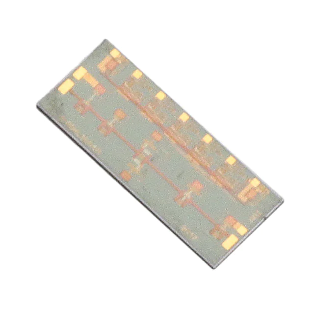
- Part No.:
- HMC941-SX
- Manufacturer:
- Analog Devices Inc.
- Category:
- Attenuators
- Package:
- Die
- Datasheet:
-
 HMC941-SX.pdf
- Description:
- IC ATTEN 0.5DB LSB DIE
- Quantity:
- Payment:

- Shipping:

Inventory:3,464
Please send an inquiry. Send us your inquiry, and we will respond immediately.
Product details
Overview
HMC941-SX from Hittite Microwave Corporation (now part of Analog Devices) is a GaAs MMIC 5-bit digital attenuator IC designed for RF signal level control in microwave front-ends. It delivers 0.5 dB LSB steps across 15.5 dB range, operates from 0.1 to 33 GHz, exhibits ±0.3 dB typical attenuation accuracy, and supports +45 dBm input IP3 - ideal for broadband test equipment and satellite transceivers.
For engineers reviewing the HMC941-SX datasheet, HMC941-SX pinout, HMC941-SX application, or HMC941-SX equivalent, key selection criteria include its 33 GHz bandwidth, 5-bit parallel control interface, 16 mm² leadless SMT package, high linearity at +45 dBm IIP3, and operation over –40°C to +85°C industrial temperature range.
Technical Context
The HMC941-SX implements a monolithic GaAs-based 5-bit switched-attenuator architecture with binary-weighted bit values (0.5/1/2/4/8 dB), enabling precise RF amplitude control via five independent TTL-compatible control lines (P0–P4). All bits are DC-coupled and referenced to Vdd = +5 V and Vss = –5 V.
It features matched 50 Ω RF ports (RF1/RF2), requires external grounding of all N/C pins and the exposed paddle, and maintains stable return loss (>12 dB) and insertion loss (<6.5 dB) across its full 0.1–33 GHz band - critical for wideband microwave systems where phase and amplitude consistency matter.
Key Specifications
| Parameter | Value and Actual Design Meaning |
|---|---|
| Frequency Range | 0.1–33.0 GHz - supports full-bandwidth operation in Ka-band radar and 5G FR2 test systems. |
| Attenuation Range & Step | 0–15.5 dB in 0.5 dB LSB increments - enables fine-grained RF power leveling without interpolation. |
| Insertion Loss | ≤4.5 dB (0.1–18 GHz), ≤6.5 dB (26.5–33 GHz) - low loss preserves system noise figure and gain budget. |
| Input IP3 | +45 dBm (0.5–33 GHz) - high linearity prevents intermodulation distortion in multi-tone environments. |
| Attenuation Accuracy | ±(0.3 + 4%) of setting (0.5–7.5 dB), ±(0.3 + 8%) (8–15.5 dB) - ensures predictable signal scaling across dynamic range. |
| Switching Speed | tRISE/tFALL ≤60 ns, tON/tOFF ≤90 ns - supports fast AGC and TDD timing in real-time RF control loops. |
| Supply Voltages | Vdd = +5 V, Vss = –5 V - dual-rail bias enables symmetric switching and low DC offset on RF path. |
Pinout & Package
Package: 24-lead 4×4 mm leadless plastic QFN (LP4) with exposed ground paddle; RoHS-compliant version available as HMC941LP4E. Requires soldering of all ground leads and paddle to PCB RF ground per Hittite land pattern guidelines.
| Pin/Terminal | Circuit Role | Design Meaning |
|---|---|---|
| 1 | Vss | Negative supply rail (–5 V); must be decoupled and grounded to minimize noise coupling into RF path. |
| 2–4, 6–13, 15–17, 19 | N/C | No internal connection; externally grounded to RF/DC ground to suppress parasitic resonance and improve shielding. |
| 5, 14 | RF1, RF2 | DC-coupled 50 Ω RF I/O ports; require external blocking capacitors if DC bias differs from 0 V. |
| 18 | Vdd | Positive supply rail (+5 V); requires local 100 nF + 10 µF decoupling near pin for stable bias under RF switching. |
| 20–24 | P0–P4 | 5-bit parallel digital control inputs; logic high = +5 V, low = 0 V; each controls one attenuation bit (0.5/1/2/4/8 dB). |
| Bottom Paddle | GND | Thermal and RF ground reference; must be fully soldered to solid PCB ground plane for thermal dissipation and impedance stability. |
Key Features
| Feature | Design Value |
|---|---|
| Ultra-wideband coverage | 0.1–33 GHz continuous operation - eliminates need for multiple narrowband attenuators in multi-band platforms. |
| High linearity | +45 dBm input IP3 at 0.5–33 GHz - maintains signal integrity in high-power receiver front-ends and transmitter calibration paths. |
| Low step error | ±0.3 dB typical bit error - ensures monotonic attenuation behavior and repeatable power control in closed-loop systems. |
| Fast digital switching | ≤90 ns enable/disable delay - compatible with LTE/NR TDD frame timing and rapid channel calibration sequences. |
| Industrial temperature range | –40°C to +85°C operation - qualified for deployment in base station radios, airborne sensors, and field-deployable test gear. |
Applications
| Fiber Optic Transmitter Calibration | Microwave Point-to-Point Radio |
|---|---|
Use Scenario: Precise optical modulation depth control in 100G+ coherent transceivers using RF-driven Mach-Zehnder modulators. IC Role / Device Role / Timing Role: Digital attenuator placed in the RF drive path to adjust modulator bias point and optimize extinction ratio. Use Value: 0.5 dB LSB resolution and ±0.3 dB accuracy enable sub-percent power tuning critical for minimizing EVM in DP-QPSK signals. |
Use Scenario: Adaptive output power control in 24–33 GHz licensed microwave backhaul radios operating in variable propagation conditions. IC Role / Device Role / Timing Role: Front-end RF attenuator in transmit chain, dynamically adjusted by baseband controller to maintain EIRP compliance. Use Value: 33 GHz bandwidth and +45 dBm IIP3 ensure linear operation across full Ka-band, avoiding compression-induced spectral regrowth. |
| Space-Qualified Satellite Payload | Automated Test Equipment (ATE) |
Use Scenario: Gain stabilization in LEO satellite telemetry downlink amplifiers subject to thermal cycling and radiation exposure. IC Role / Device Role / Timing Role: Radiation-tolerant (Class 1A ESD) attenuator used in closed-loop AGC circuit to compensate for PA drift over orbit. Use Value: –40°C to +85°C rating and 16 mm² hermetic-grade LP4 package support long-term reliability in vacuum and thermal vacuum environments. |
Use Scenario: Programmable RF stimulus level generation in vector network analyzers and signal analyzers requiring traceable, repeatable attenuation. IC Role / Device Role / Timing Role: Digitally controlled attenuation stage in calibrated RF source module, synchronized with instrument sweep timing. Use Value: 60 ns rise/fall time and 5-bit parallel interface allow microsecond-level attenuation updates during fast frequency sweeps. |
Equivalent & Alternatives
The following parts are listed as comparable options for similar digital RF attenuator applications.
| Alternative Part | Technical Difference | Application Difference | Selection Advice |
|---|---|---|---|
| HMC624LP4 | 4-bit, 0.5 dB LSB, 0.1–20 GHz, +42 dBm IIP3, same LP4 package | Limited to 20 GHz; lower linearity; suitable for sub-20 GHz telecom infrastructure | Select when bandwidth and IP3 requirements are relaxed and cost sensitivity is higher. |
| PE43711 | 6-bit, 0.25 dB LSB, 0.01–8 GHz, +41 dBm IIP3, 24-pin QFN | Narrower bandwidth (≤8 GHz); finer resolution; optimized for cellular and WiFi bands | Prefer for sub-6 GHz wireless test systems needing <0.5 dB step granularity and lower frequency stability. |
Compared with HMC624LP4 and PE43711, the HMC941-SX uniquely combines 33 GHz bandwidth, +45 dBm IIP3, and 5-bit 0.5 dB resolution - making it the only option among the three qualified for Ka-band radar calibration and space-grade wideband instrumentation.
Availability
HMC941-SX is available at Aetrix Electronics and suitable for fiber optic transceivers, microwave radio links, satellite communication payloads, and automated test equipment requiring stable component supply across extended temperature and frequency ranges.
Supply support for HMC941-SX includes scheduled delivery planning, volume procurement assistance, BOM continuity management, traceable sourcing, and lifecycle availability coordination for OEM customers, industrial embedded developers, connected-device designers, and electronics production programs.
Manufacturer
Hittite Microwave Corporation, acquired by Analog Devices in 2014, specialized in high-frequency RFICs and MMICs for defense, aerospace, and communications markets.
The HMC941-SX belongs to Hittite's broadband GaAs digital attenuator product line, engineered for ultra-wideband RF power control in mission-critical microwave systems where bandwidth, linearity, and repeatability are non-negotiable.
FAQ
What is the operating frequency range of the HMC941-SX?
The HMC941-SX operates continuously from 0.1 GHz to 33.0 GHz. Its insertion loss remains below 6.5 dB across this entire band, with specified performance validated at key points including 18 GHz, 26.5 GHz, and 33 GHz - making it suitable for Ka-band radar, satellite uplinks, and millimeter-wave test instrumentation where wide instantaneous bandwidth is essential.
Does the HMC941-SX require external DC blocking capacitors?
Yes, the HMC941-SX RF1 and RF2 ports are DC-coupled and internally matched to 50 Ω. If the connected RF line carries non-zero DC potential, external blocking capacitors must be placed in series with both ports to prevent bias disruption and ensure proper 50 Ω termination. Typical values used in evaluation boards are 1000 pF in 0402 package.
What are the absolute maximum ratings for Vdd and Vss on the HMC941-SX?
The HMC941-SX has absolute maximum ratings of +7 Vdc for Vdd and –7 Vdc for Vss. The recommended operating bias is +5 V for Vdd and –5 V for Vss, drawing 2.5–6.5 mA and –3.0 to –7.0 mA respectively. Exceeding these limits risks permanent damage to the GaAs die or bond wires.
Is the HMC941-SX pin-compatible with the HMC941LP4 or HMC941LP4E?
Yes - HMC941-SX is the die-on-carrier or bare-die variant corresponding to the packaged HMC941LP4 (Sn/Pb) and HMC941LP4E (100% matte Sn) versions. All share identical pinout, electrical specifications, and functional behavior; the "-SX" suffix denotes the unpackaged form intended for hybrid assembly or custom packaging.
How is attenuation accuracy specified across the full range of the HMC941-SX?
Attenuation accuracy for the HMC941-SX is specified as ±(0.3 + 4%) of the set attenuation value for states from 0.5 dB to 7.5 dB, and ±(0.3 + 8%) for states from 8 dB to 15.5 dB - measured at 25°C with Vdd = +5 V and Vss = –5 V. This reflects both fixed offset and proportional error components inherent to GaAs switched-attenuator topology.
HMC941-SX Specifications
- Product attributes
- Attribute value
- Manufacturer:
- Analog Devices Inc.
- Package/Case:
- Die
- Series:
- -
- Packaging:
- Bulk
- Product Status:
- Obsolete
- Attenuation Value:
- 15.5dB
- Frequency Range:
- 100 MHz ~ 30 GHz
- Power (Watts):
- -
- Impedance:
- 50 Ohms
- Grade:
- -
- Qualification:
- -
HMC941-SX FAQ
1.How can I place an order for HMC941-SX through Aetrix?
Please submit a Request for Quotation (RFQ) for HMC941-SX on Aetrix. Our sales agent will provide a competitive quotation and guide you through the order confirmation once you accept the terms.
2.Are the price and stock information for HMC941-SX reliable?
The price and inventory of HMC941-SX are updated periodically and may fluctuate due to market conditions. Stock and pricing data are typically refreshed every 24 hours. Quotation validity for HMC941-SX is usually 5 days.
3.What payment methods are accepted for HMC941-SX?
We accept Wire Transfer, PayPal, Credit Card, Western Union, MoneyGram, and Escrow for HMC941-SX transactions.
Note: Certain payment methods may incur a processing fee.
4.How is shipping managed for HMC941-SX?
HMC941-SX orders can be shipped via leading logistics carriers, including DHL, UPS, FedEx, TNT, or Registered Mail.
Once your HMC941-SX order is processed, you will receive an email with the shipment details and tracking number.
Note: Tracking information may take up to 24 hours to appear. Express delivery typically takes 3–5 business days.
5.How can I obtain technical support or documentation for HMC941-SX?
For technical support, including HMC941-SX datasheets, pinout diagrams, or application guidance, please contact our engineering support team. They can provide detailed documentation and assistance for your HMC941-SX requirements.
6.How does Aetrix verify that HMC941-SX is sourced from the original manufacturer or authorized distributors?
All HMC941-SX products on Aetrix are procured from qualified distributors and authorized channels. Our dedicated quality assurance team conducts strict verification, including traceability checks and, if necessary, third-party testing. This ensures that HMC941-SX meets industry standards.
7.What is the process for return or replacement of HMC941-SX?
All HMC941-SX units undergo pre-shipment inspection (PSI). If there is an issue with HMC941-SX, returns or replacements are accepted under the following conditions:
1.Quantity discrepancies, incorrect items, or visible external defects (such as breakage or corrosion), acknowledged by Aetrix.
2.The issue is reported within 90 days of delivery.
3.The HMC941-SX part is unused and in its original packaging.
Return procedure for HMC941-SX:
1.Submit a request within 90 days.
2.Obtain a Return Material Authorization (RMA) from Aetrix.
HMC941-SX Tags

-
PAT0510S-C-3DB-T10
Susumu
-
PAT0510S-C-10DB-T10
Susumu
-
PAT0510S-C-2DB-T10
Susumu
-
PAT1220-C-10DB-T5
Susumu
-
PAT1220-C-6DB-T5
Susumu
-
PAT1220-C-0DB-T5
Susumu
-
PAT1220-C-3DB-T5
Susumu
-
PAT1220-C-5DB-T5
Susumu
-
PAT1220-C-8DB-T5
Susumu
-
MAADSS0008TR-3000
MACOM Technology Solutions
-
MAATSS0018TR-3000
MACOM Technology Solutions
-
PE43205B-Z
pSemi
Tech Hub

A practical engineering guide to 3.3V and 5V logic compatibility, input thresholds, resistor dividers, translator ICs, MOSFET level shifting, I2C pull-ups, timing limits and power-sequencing risks.

The 74HC595 uses push-pull logic outputs, while the TPIC6B595 uses 50 V open-drain DMOS sinks for higher-power loads. This guide compares timing, current limits, 3.3 V interfacing, load wiring, thermal…

The 74HC595 converts serial data into eight stable parallel outputs. This guide covers pin functions, shift and storage timing, OE and MR behavior, drive-current limits, cascading, voltage compatibilit…

A technical comparison of level-sensitive latches and edge-triggered flip-flops, covering timing windows, setup and hold limits, master–slave operation, time borrowing, race-through, HDL inference and…

A D latch stores one bit while Enable controls when data can pass. This reference covers gate-level operation, truth tables, transparency, setup and hold timing, LE versus OE, common ICs and practical …

An SR latch stores one bit through cross-coupled feedback. This engineering reference covers NOR and NAND implementations, truth tables, forbidden-state recovery, gated operation, switch debouncing, fa…

Latch circuits retain one bit through feedback. This technical reference covers SR and D latches, truth tables, transparency, timing limits, latch-versus-flip-flop behavior, applications and common log…

An engineering guide to LED driver operation, constant-current and constant-voltage outputs, linear and switching topologies, dimming, IC selection, calculations, replacement compatibility, and fault c…

Operational amplifier guide covering op amp basics, feedback, ideal vs real op amps, common configurations, buffer circuits, offset, bias current, gain-bandwidth, slew rate, rail-to-rail limits and sel…

Jumper cables guide covering safe connection order, red and black clamp placement, final ground connection, cable gauge, length, clamp quality, copper vs CCA cables, jump starter comparison and battery…


