
 My Inquiry
 My Account


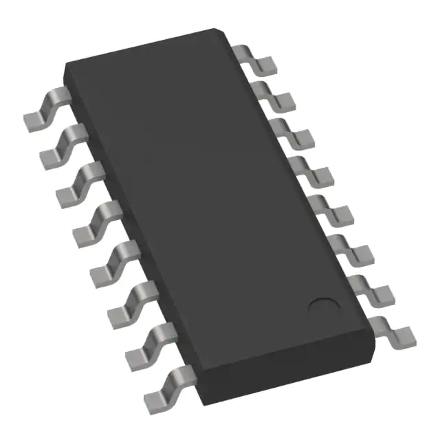
Monolithic Power Systems Inc. HR1001LGS-Z
- Part No.:
- HR1001LGS-Z
- Manufacturer:
- Monolithic Power Systems Inc.
- Category:
- Power Supply Controllers, Monitors
- Package:
- 16-SOIC (0.154", 3.90mm Width)
- Datasheet:
-
 HR1001LGS-Z.pdf
- Description:
- IC ENHANCED LLC CONTROLLR 16SOIC
- Quantity:
- Payment:

- Shipping:

Inventory:1,842
Please send an inquiry. Send us your inquiry, and we will respond immediately.
Product details
Overview
HR1001LGS-Z from Monolithic Power Systems is an enhanced LLC resonant half-bridge controller featuring adaptive dead-time adjustment (ADTA), capacitive mode protection (CMP), two-level over-current protection (OCP), programmable burst mode, and a high-accuracy oscillator with dV/dt immunity. It delivers 50% duty cycle, variable-frequency control up to 600 kHz, and integrates 600 V high-side gate drivers with bootstrap diode. Used in high-efficiency AC/DC power supplies for LCD TVs and telecom SMPS.
For engineers reviewing the HR1001LGS-Z datasheet, HR1001LGS-Z pinout, HR1001LGS-Z application, or HR1001LGS-Z equivalent, key selection criteria include ADTA-enabled ZVS optimization across load range, CMP response time (52 µs), dual-threshold OCP (0.78 V / 1.5 V), SOIC-16 thermal performance (θJA = 80 °C/W), and HBVS dV/dt sensing interface for real-time dead-time tuning.
Technical Context
The HR1001LGS-Z implements a resonant control architecture where the CT/FSET oscillator sets min/max switching frequency (e.g., 60–200 kHz) via external R-C networks, while ADTA dynamically adjusts dead time between HG and LG outputs based on SW node dV/dt sensed through HBVS and CHBVS (5 pF typical). Its current-sense path (CS) enables both frequency-shift OCP and latch-off protection.
Capacitive mode protection operates by comparing CS voltage against polarity thresholds (VCSPR = 50–131 mV, VCSNR = –131 to –50 mV) after each gate transition, triggering a 52 µs timer before SS discharge - preventing destructive shoot-through during overload. The IC enters controlled burst mode when BURST pin voltage falls below 1.23 V, reducing quiescent current to 1.2 mA at light load.
Key Specifications
| Parameter | Value and Actual Design Meaning |
|---|---|
| Switching frequency range | Programmable 60 kHz to 600 kHz; sets resonant tank operating point and efficiency envelope. |
| Adaptive dead time | 235–1000 ns; dynamically tuned via HBVS dV/dt sensing to maintain ZVS across load and line conditions. |
| OCP thresholds | 0.78 V (frequency shift) and 1.5 V (latch-off); enables staged fault response without immediate shutdown. |
| Capacitive mode timer | 52 µs fixed delay before SS discharge; ensures robust detection of capacitive conduction before action. |
| Gate drive capability | HG/LG: 0.74 A source / 0.87 A sink peak; drives standard 10–20 nC MOSFETs in half-bridge topology. |
| HBVS dV/dt sensitivity | Detects ≥180 V/µs; determines minimum usable CHBVS capacitor (e.g., 5 pF) for reliable ADTA operation. |
| Burst mode threshold | 1.23 V ±30 mV on BURST pin; initiates low-power idle state to reduce no-load consumption. |
| SOIC-16 thermal resistance | θJA = 80 °C/W; defines maximum power dissipation (1.56 W at TA = 25°C) before thermal shutdown. |
Pinout & Package
HR1001LGS-Z is housed in a standard SOIC-16 package with creepage-enhancing NC pin (Pin 13) and integrated bootstrap diode. Pin functions are validated per MPS HR1001L Rev.1.0 datasheet (April 2016).
| Pin/Terminal | Circuit Role | Design Meaning |
|---|---|---|
| 1 SS | Soft-start timing node | Controls exponential frequency ramp-up via external R-C; discharges internally during fault to ensure monotonic VOUT rise. |
| 2 TIMER | OCP duration timer | Charged by 130 µA current source when CS > 0.78 V; triggers latch at 3.5 V, resets only after VCC UVLO cycle. |
| 3 CT | Oscillator timing capacitor | Charged/discharged between 0.9 V and 3.8 V by FSET-programmed current; defines switching frequency base. |
| 4 FSET | Frequency set reference | 2.0 V ±3% internal reference; resistor to GND sets min frequency; optocoupler feedback modulates max frequency. |
| 5 BURST | Burst mode enable | Compares to 1.23 V reference; disables switching and reduces IQ to 1.2 mA when below threshold. |
| 6 CS | Primary current sense input | Dual-function: OCP detection (0.78 V / 1.5 V) and CMP polarity comparison (±50–131 mV) with blanking. |
| 7 BO | Line voltage monitor | Enables driver above 2.4 V, disables below 1.81 V; provides brown-in/brown-out protection with 2.8 V hysteresis. |
| 8 LATCH | External fault latch | High-impedance input; latches off IC when >1.85 V; reset requires full VCC UVLO cycle. |
| 9 HBVS | dV/dt sensing node | Connects to SW via 5 pF capacitor; detects slope polarity to trigger ADTA logic and prevent shoot-through. |
| 10 GND | Signal and power return | Common reference for LG driver, bias circuitry, and analog inputs; requires separate pulsed-current trace. |
| 11 LG | Low-side gate driver output | 0.87 A sink / 0.75 A source; referenced to GND; pulls low during UVLO. |
| 12 VCC | Supply and bias rail | 13–15.5 V operating range; powers IC core and LG driver; clamped at 16.5 V. |
| 13 NC | No-connect spacer | Internal open; isolates BST/SW pins for safety creepage compliance on PCB layout. |
| 14 SW | High-side source return | Switching node return for HG driver; requires low-inductance layout to minimize ringing. |
| 15 HG | High-side floating gate driver | 0.87 A sink / 0.74 A source; referenced to SW; includes internal pull-down during UVLO. |
| 16 BST | Bootstrap supply | Charged via internal diode from LG; supplies HG driver; requires 0.1 µF ceramic capacitor to SW. |
Key Features
| Feature | Design Value |
|---|---|
| Adaptive Dead-Time Adjustment (ADTA) | Eliminates fixed dead-time tuning effort by auto-adjusting 235–1000 ns based on real-time SW dV/dt, preserving ZVS across 0–100% load. |
| Capacitive Mode Protection (CMP) | Prevents destructive shoot-through during short-circuit by detecting current polarity reversal at CS and enforcing 52 µs blanking before action. |
| Two-Level Over-Current Protection | First-stage frequency shift (at 0.78 V) limits power gradually; second-stage latch-off (at 1.5 V) halts operation until VCC recycle. |
| Non-linear Soft Start | Exponential frequency ramp via SS RC network ensures monotonic VOUT rise and avoids inrush-induced transformer saturation. |
| 600 V High-Side Gate Driver | Integrates bootstrap diode and supports direct drive of 600 V MOSFETs without external high-voltage level shifters. |
| Programmable Burst Mode | Reduces standby power by lowering IQ to 1.2 mA when load drops below threshold, improving no-load efficiency in adapter applications. |
Applications
| LCD TV Power Supply | Telecom SMPS |
|---|---|
Use Scenario: 24 V/100 W resonant half-bridge converter powering LCD backlight and logic rails in 4K TV sets. IC Role / Device Role / Timing Role: Primary-side LLC controller regulating output via FSET optocoupler feedback; manages ZVS transitions using ADTA and prevents capacitive failure during hot-plug events. Use Value: Enables >94% peak efficiency and <0.5 W no-load consumption via burst mode, meeting Energy Star v7 standby requirements. | Use Scenario: 48 V/300 W front-end AC/DC module for telecom base station power distribution. IC Role / Device Role / Timing Role: Resonant controller synchronizing with upstream PFC stage; uses BO pin for brown-out ride-through and LATCH for system-level fault isolation. Use Value: Delivers 125°C junction operation with θJA = 80 °C/W, supporting convection-cooled telecom chassis without forced air. |
| Desktop PC ATX PSU | AC/DC Adapter |
Use Scenario: +12 V main rail LLC stage in 80 PLUS Titanium-certified ATX power supply. IC Role / Device Role / Timing Role: Controls dual-phase half-bridge with precise 50% duty cycle; leverages SS pin for inrush-limited cold start under full capacitive load. Use Value: Achieves <1% output regulation error across line/load via FSET feedback modulation and non-linear soft start. | Use Scenario: 19 V/65 W universal-input adapter for ultrabooks with USB-C PD negotiation. IC Role / Device Role / Timing Role: Standalone LLC controller managing variable-frequency regulation; uses BURST pin to meet DOE Level VI 0.1 W no-load limit. Use Value: Reduces adapter no-load power to 85 mW via programmable burst threshold and sub-1.5 mA quiescent current. |
Equivalent & Alternatives
The following parts are listed as comparable options for similar LLC controller applications.
| Alternative Part | Technical Difference | Application Difference | Selection Advice |
|---|---|---|---|
| UCC256301DR | Integrated 600 V gate drivers omitted; requires external high-side driver; fixed 500 kHz max frequency. | Lacks ADTA and CMP; relies on external dV/dt sensing and discrete protection logic. | Choose for cost-sensitive designs where ADTA complexity is unnecessary and external driver integration is acceptable. |
| ICE2HS01G | Fixed dead time (250 ns); no dV/dt sensing; OCP only at single threshold (1.2 V); no burst mode. | No capacitive mode detection; limited light-load efficiency due to fixed-frequency operation. | Select when designing legacy half-bridge systems with stable load profiles and no requirement for adaptive ZVS. |
Compared with UCC256301DR and ICE2HS01G, the HR1001LGS-Z uniquely combines ADTA, CMP, and dual-threshold OCP in a single SOIC-16 package-enabling robust ZVS across wide load ranges without external sensing components or protection ICs.
Availability
HR1001LGS-Z is available at Aetrix Electronics and suitable for LCD TV power supplies, telecom SMPS, and desktop PC ATX PSUs requiring stable component supply, long-term lifecycle support, and RoHS-compliant manufacturing.
Supply support for HR1001LGS-Z includes scheduled delivery planning, volume procurement assistance, BOM continuity management, traceable sourcing, and lifecycle availability coordination for OEM customers, industrial embedded developers, connected-device designers, and electronics production programs.
Manufacturer
Monolithic Power Systems (MPS) is a fabless semiconductor company specializing in high-performance analog and power ICs, with design centers in the US, China, and Taiwan.
The HR1001L product line targets high-efficiency resonant AC/DC conversion, specifically engineered for LLC half-bridge topologies in consumer, computing, and telecom power supplies where ZVS reliability and light-load efficiency are critical.
FAQ
What is the purpose of the HBVS pin and how is it used?
The HBVS pin senses dV/dt at the SW node via an external capacitor (typically 5 pF) to enable Adaptive Dead-Time Adjustment. When SW transitions, current through CHBVS pulls HBVS voltage down; the IC uses this signal to dynamically adjust dead time between HG and LG outputs, ensuring zero-voltage switching across load conditions without manual tuning.
How does capacitive mode protection (CMP) operate during overload?
CMP monitors CS voltage polarity after each gate transition. If CS crosses VCSPR (50–131 mV) after HG turns off or VCSNR (–131 to –50 mV) after LG turns off, the IC starts a 52 µs timer. If polarity remains invalid after timeout, SS discharges to raise frequency and limit energy-preventing shoot-through before hard fault escalation.
Can HR1001LGS-Z be used without connecting the HBVS pin?
Yes, but ADTA is disabled. Without HBVS connection, dead time defaults to fixed 350 ns. While functional, this eliminates ZVS optimization at light loads and increases risk of hard switching or efficiency loss-especially with large magnetizing inductance or wide input voltage range.
What is the role of the TIMER pin in over-current handling?
The TIMER pin implements a timed OCP response: when CS exceeds 0.78 V, a 130 µA current charges the external TIMER capacitor. If voltage reaches 3.5 V, the IC latches off. Recovery requires both TIMER voltage falling below 0.28 V and a full VCC UVLO cycle-ensuring faults are not cleared prematurely.
How is burst mode triggered and what is its impact on efficiency?
Burst mode activates when voltage on the BURST pin falls below 1.23 V (±30 mV hysteresis), causing the IC to halt switching and reduce quiescent current to 1.2 mA. This cuts no-load power consumption significantly-e.g., enabling <0.1 W adapters-while maintaining fast wake-up (<100 µs) when load returns.
What are the absolute maximum ratings for SW and BST pins?
The SW pin withstands –3 V to 600 V with a maximum dV/dt of 50 V/ns; the BST pin handles –0.3 V to 618 V. Exceeding these may damage internal structures. Layout must minimize SW node inductance and use low-ESR/ESL BST capacitors to avoid voltage overshoot beyond 600 V during transients.
Is the HR1001LGS-Z RoHS and halogen-free compliant?
Yes. HR1001LGS-Z is lead-free, halogen-free, and fully compliant with EU RoHS Directive 2011/65/EU. MPS confirms green status on its Quality Assurance portal, and all packaging materials meet IEC 61249-2-21 standards for brominated flame retardants.
HR1001LGS-Z Specifications
- Product attributes
- Attribute value
- Manufacturer:
- Monolithic Power Systems Inc.
- Series:
- -
- Package/Case:
- 16-SOIC (0.154", 3.90mm Width)
- Packaging:
- Tape & Reel (TR)
- Product Status:
- Active
- Programmable:
- -
- Applications:
- Flyback, Forward Converters, LLC
- Voltage - Input:
- -0.3V ~ 6V
- Voltage - Supply:
- 13V ~ 15.5V
- Current - Supply:
- 3 mA
- Operating Temperature:
- -40°C ~ 125°C (TJ)
- Grade:
- -
- Qualification:
- -
- Mounting Type:
- Surface Mount
- Supplier Device Package:
- 16-SOIC
HR1001LGS-Z FAQ
1.How can I place an order for HR1001LGS-Z through Aetrix?
Please submit a Request for Quotation (RFQ) for HR1001LGS-Z on Aetrix. Our sales agent will provide a competitive quotation and guide you through the order confirmation once you accept the terms.
2.Are the price and stock information for HR1001LGS-Z reliable?
The price and inventory of HR1001LGS-Z are updated periodically and may fluctuate due to market conditions. Stock and pricing data are typically refreshed every 24 hours. Quotation validity for HR1001LGS-Z is usually 5 days.
3.What payment methods are accepted for HR1001LGS-Z?
We accept Wire Transfer, PayPal, Credit Card, Western Union, MoneyGram, and Escrow for HR1001LGS-Z transactions.
Note: Certain payment methods may incur a processing fee.
4.How is shipping managed for HR1001LGS-Z?
HR1001LGS-Z orders can be shipped via leading logistics carriers, including DHL, UPS, FedEx, TNT, or Registered Mail.
Once your HR1001LGS-Z order is processed, you will receive an email with the shipment details and tracking number.
Note: Tracking information may take up to 24 hours to appear. Express delivery typically takes 3–5 business days.
5.How can I obtain technical support or documentation for HR1001LGS-Z?
For technical support, including HR1001LGS-Z datasheets, pinout diagrams, or application guidance, please contact our engineering support team. They can provide detailed documentation and assistance for your HR1001LGS-Z requirements.
6.How does Aetrix verify that HR1001LGS-Z is sourced from the original manufacturer or authorized distributors?
All HR1001LGS-Z products on Aetrix are procured from qualified distributors and authorized channels. Our dedicated quality assurance team conducts strict verification, including traceability checks and, if necessary, third-party testing. This ensures that HR1001LGS-Z meets industry standards.
7.What is the process for return or replacement of HR1001LGS-Z?
All HR1001LGS-Z units undergo pre-shipment inspection (PSI). If there is an issue with HR1001LGS-Z, returns or replacements are accepted under the following conditions:
1.Quantity discrepancies, incorrect items, or visible external defects (such as breakage or corrosion), acknowledged by Aetrix.
2.The issue is reported within 90 days of delivery.
3.The HR1001LGS-Z part is unused and in its original packaging.
Return procedure for HR1001LGS-Z:
1.Submit a request within 90 days.
2.Obtain a Return Material Authorization (RMA) from Aetrix.
HR1001LGS-Z Tags

-
UC3845AD8TR
Texas Instruments
-
UC2843AD8TR
Texas Instruments

-
LM3880MFX-1AE/NOPB
Texas Instruments
-
LM3880MFX-1AA/NOPB
Texas Instruments
-
INA234AIYBJR
Texas Instruments

-
INA700AYWFR
Texas Instruments
-
LM3880MF-1AE/NOPB
Texas Instruments
-
LM3880MF-1AA/NOPB
Texas Instruments
-
LM3881MM/NOPB
Texas Instruments
-
UCC2802DTR
Texas Instruments
-
NCP4305DMTTWG
onsemi
-
INA237AIDGSR
Texas Instruments
Tech Hub

Operational amplifier guide covering op amp basics, feedback, ideal vs real op amps, common configurations, buffer circuits, offset, bias current, gain-bandwidth, slew rate, rail-to-rail limits and sel…

Jumper cables guide covering safe connection order, red and black clamp placement, final ground connection, cable gauge, length, clamp quality, copper vs CCA cables, jump starter comparison and battery…

LDO regulator guide covering low dropout voltage, power dissipation, thermal design, PSRR, output noise, capacitor stability, adjustable LDO circuits, LDO vs buck converter and datasheet selection chec…

Conditional Access Module guide covering CAM meaning, CI/CI+ interface, smart card authorization, DVB security workflow, TV and set-top box compatibility, internal electronics, ESD protection, connecto…

Guide to electronic component obsolescence covering EOL risk, PCN/PDN notices, last-time buy planning, replacement options, form-fit-function validation, counterfeit risk and BOM lifecycle management.

18650 battery guide covering lithium-ion cell basics, 3.6V/3.7V voltage, 4.2V charging, mAh and Wh capacity, protected cells, chargers, BMS, series-parallel packs, holders, welding and sourcing checks.…

Hall effect sensor guide covering working principle, linear and digital sensors, Arduino circuits, current sensing, speed detection, automotive applications, A3144 examples, signal filtering and datash…

Product Change Notification guide for electronic components, covering PCN meaning, PCN vs PDN/EOL, common change types, risk levels, form-fit-function review, engineering validation, BOM control, LTB/L…

A practical guide to blend door actuators, covering HVAC function, symptoms, location, AC and heater issues, reset and calibration, replacement cost, electrical diagnosis, compatibility checks, and rep…

Engineering guide to Raspberry Pi alternatives, covering chip-level differences, Orange Pi, ROCK, Jetson, Banana Pi, NanoPi, Compute Module, Pico, GPIO, camera, HAT compatibility, and replacement risks…


