
 My Inquiry
 My Account


Renesas HSP45102SC-40Z
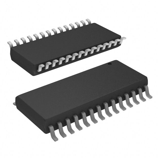
- Part No.:
- HSP45102SC-40Z
- Manufacturer:
- Renesas
- Category:
- Programmable Timers and Oscillators
- Package:
- 28-SOIC (0.295", 7.50mm Width)
- Datasheet:
-
 HSP45102SC-40Z.pdf
- Description:
- IC OSC NCO 40MHZ 28-SOIC
- Quantity:
- Payment:

- Shipping:

Inventory:4,720
Please send an inquiry. Send us your inquiry, and we will respond immediately.
Product details
Overview
HSP45102SC-40Z from Intersil is a 12-bit numerically controlled oscillator (NCO) with 32-bit frequency resolution, 40MHz maximum clock rate, and offset-binary 12-bit sine-wave output. It implements direct digital synthesis for precise frequency generation in communications systems, supporting BFSK/QPSK modulation via dual 32-bit frequency words and 90°-increment phase control through P0–P1 inputs.
For engineers reviewing the HSP45102SC-40Z datasheet, HSP45102SC-40Z pinout, HSP45102SC-40Z application, or HSP45102SC-40Z equivalent, key selection criteria include its 0.009Hz tuning resolution at 40MHz, -69dBc spurious performance, single-cycle frequency switching, and serial frequency loading architecture with pipeline-controlled timing.
Technical Context
The HSP45102SC-40Z integrates a 64-bit bidirectional shift register for serial frequency word loading, selectable MSB/LSB-first shifting, and dual 32-bit word selection via SEL_L/M. Its phase accumulator advances using integer arithmetic per Equation 2 (fOUT = fCLK × N / 232), with 13-bit phase angle computation feeding a Sine ROM.
Phase modulation is implemented by adding encoded P0–P1 bits to the top two bits of the 13-bit phase accumulator output, enabling 0°/90°/180°/270° shifts mapped directly to QPSK I/Q data paths. Output is delivered as offset-binary 12-bit data (OUT0–OUT11), compatible with standard DAC interfaces without sign-extension logic.
Key Specifications
| Parameter | Value and Actual Design Meaning |
|---|---|
| Max Clock Frequency | 40MHz - Enables output frequency synthesis up to ~10MHz with full 32-bit resolution and <0.009Hz step size. |
| Frequency Resolution | 0.009Hz at 40MHz - Achieved via 32-bit tuning word; supports fine-grained channel spacing in narrowband radios. |
| Spurious Free Dynamic Range | <-69dBc - Ensures clean spectral purity critical for PSK demodulation and low-error-rate communication links. |
| Output Format | 12-bit offset binary (OUT0=LSB) - Simplifies interface to 12-bit DACs (e.g., HI5731) without external level-shifting or biasing. |
| Phase Modulation | P0–P1 inputs enable 0°/90°/180°/270° shifts - Directly supports QPSK symbol mapping without external XOR logic or lookup tables. |
| Frequency Switching Latency | 1 clock cycle + 6-cycle pipeline delay - Allows rapid hop-settling in frequency-hopping spread spectrum (FHSS) systems. |
| Supply Voltage | +4.75V to +5.25V - Compatible with standard 5V TTL/CMOS logic rails and industrial-grade power supplies. |
Pinout & Package
Package: 28-lead SOIC (300 mil), Pb-free (RoHS compliant), M28.3 footprint (17.70–18.10 mm × 7.40–7.60 mm).
| Pin/Terminal | Circuit Role | Design Meaning |
|---|---|---|
| VCC | Power supply input | +5V rail connection; requires local 0.1µF decoupling per datasheet layout guidelines. |
| GND | Ground reference | Dual ground pins (pins 8, 15) reduce noise coupling between analog and digital sections. |
| CLK | Master system clock input | CMOS-level 40MHz clock; timing-critical path governing all internal pipeline stages. |
| SCLK | Serial shift clock | Rising-edge-triggered clock for frequency word loading; independent of CLK domain. |
| SD | Serial data input | MSB/LSB-first data stream into 64-bit frequency register; synchronized to SCLK when SFTEN low. |
| SFTEN | Shift enable (active low) | Gate controlling data entry into frequency register; must be held low during full 64-bit load sequence. |
| MSB/LSB | Shift direction control | Selects bit-order: high = MSB-first (data enters at FRCTRL63); low = LSB-first (enters at FRCTRL0). |
| SEL_L/M | Frequency word select | High = use FRCTRL0–31; low = use FRCTRL32–63; enables dual-frequency hopping without reprogramming. |
| TXFR | Transfer enable (active low) | Latches selected 32-bit word into phase accumulator input register on next CLK edge after 4-cycle pipeline delay. |
| LOAD | Phase accumulator reset | Zeroes accumulator feedback path after 5-cycle pipeline delay; used for deterministic phase initialization. |
| ENPHAC | Phase accumulator enable | Active-low gate; halts phase advancement when high, preserving current phase angle for hold modes. |
| P0, P1 | Phase modulation inputs | Encoded 2-bit control for 0°/90°/180°/270° phase offsets; active after 4-clock pipeline delay. |
| OUT0–OUT11 | 12-bit sine amplitude output | Offset-binary format (0x001–0xFFF centered at 0x800); OUT0 = LSB, OUT11 = MSB; drives DAC directly. |
Key Features
| Feature | Design Value |
|---|---|
| 32-bit frequency control resolution | Enables sub-Hz frequency steps at 40MHz clock, eliminating need for external PLL multipliers in precision signal sources. |
| Serial frequency loading interface | Reduces PCB routing complexity vs parallel bus; supports daisy-chaining multiple NCOs using shared SCLK/SD lines. |
| QPSK/BFSK modulation support | Integrated P0–P1 phase encoding and dual-word selection eliminate external modulator ICs in digital radio transceivers. |
| Offset-binary output format | Eliminates need for external DAC biasing circuitry or digital offset compensation in 12-bit DAC interfacing. |
| Static CMOS process | Permits zero-power standby (ICCSB ≤ 500µA) and glitch-free operation during clock gating or frequency hold modes. |
Applications
| Direct Digital Synthesis | QPSK Modulator |
|---|---|
|
Use Scenario: Programmable RF signal source in lab-grade function generators requiring stable, jitter-free sine outputs across 1Hz–10MHz range. IC Role / Device Role / Timing Role: Core DDS engine generating digitally defined sine wave; replaces analog VCO-based architectures with superior frequency agility and repeatability. Use Value: Delivers 0.009Hz tuning resolution and <-69dBc spurs without external filtering, reducing BOM count and calibration overhead. |
Use Scenario: I/Q baseband modulator in L-band satellite terminal transmitters implementing QPSK with real-time symbol rate adaptation. IC Role / Device Role / Timing Role: Generates phase-coherent I and Q carrier components; P0–P1 pins map directly to symbol encoder outputs for 90°-shifted carriers. Use Value: Eliminates discrete XOR gates and analog phase-shift networks, cutting latency by 6+ cycles versus FPGA-based modulators. |
| Frequency-Hopping Radio | Low-Cost Digital Radio Transceiver |
|
Use Scenario: Military/commercial FHSS radio operating in ISM bands where rapid, deterministic frequency switching (<100ns effective latency) is mandated. IC Role / Device Role / Timing Role: Frequency synthesizer core; dual 32-bit words preloaded for hop set, switched in one CLK cycle via SEL_L/M. Use Value: Achieves hop-to-hop settling in ≤6 clock cycles (150ns @ 40MHz), meeting MIL-STD-188-114B timing constraints without external PLL lock detection. |
Use Scenario: Consumer-grade digital radio (e.g., DAB, DRM) requiring low-BOM, single-chip RF synthesis with integrated modulation capability. IC Role / Device Role / Timing Role: Combined oscillator and modulator; replaces separate crystal oscillator, PLL, and analog modulator stages. Use Value: Reduces component count by ≥7 parts (VCO, loop filter, dividers, mixers, phase shifter) while improving EMI performance via digital-only signal path. |
Equivalent & Alternatives
The following parts are listed as comparable options for similar numerically controlled oscillator applications.
| Alternative Part | Technical Difference | Application Difference | Selection Advice |
|---|---|---|---|
| AD9833BRMZ-REEL | 10-bit output, 25MHz max clock, SPI interface, no phase modulation pins | Lacks P0–P1 phase control and dual-word selection; limited to basic DDS without native QPSK support | Choose AD9833BRMZ-REEL only if 10-bit resolution and absence of phase modulation are acceptable for non-PSK applications. |
| MAX2748ETL+ | Integrated VCO+PLL, 2.4GHz RF output, no digital modulation interface | Generates RF directly but lacks programmable baseband modulation; not a drop-in replacement for DDS functions | Choose MAX2748ETL+ only when RF output at GHz frequencies is required and digital baseband synthesis is unnecessary. |
Compared with AD9833BRMZ-REEL and MAX2748ETL+, the HSP45102SC-40Z uniquely delivers 12-bit resolution, 40MHz clocking, and hardware-accelerated QPSK modulation in a single SOIC package-enabling higher spectral purity and lower system latency than either alternative in digital radio baseband designs.
Availability
HSP45102SC-40Z is available at Aetrix Electronics and suitable for digital radio transceivers, satellite communication terminals, and programmable function generators requiring stable component supply with RoHS-compliant packaging and commercial temperature range (0°C to +70°C).
Supply support for HSP45102SC-40Z includes scheduled delivery planning, volume procurement assistance, BOM continuity management, traceable sourcing, and lifecycle availability coordination for OEM customers, industrial embedded developers, connected-device designers, and electronics production programs.
Manufacturer
Intersil Corporation (now part of Renesas Electronics) is a U.S.-based semiconductor designer specializing in precision analog, power management, and timing solutions for industrial, aerospace, and communications markets.
The HSP45102SC-40Z belongs to Intersil's Numerically Controlled Oscillator (NCO) product line, engineered specifically for cost-sensitive, high-accuracy digital radio and test equipment applications requiring integrated modulation and minimal external components.
FAQ
What is the maximum clock frequency supported by the HSP45102SC-40Z?
The HSP45102SC-40Z supports a maximum clock frequency of 40MHz, as confirmed by AC Electrical Specifications on page 7 of FN2810 Rev 9.00. At this rate, it achieves 0.009Hz tuning resolution and maintains <-69dBc spurious performance. Exceeding 40MHz violates absolute timing margins and may cause metastability in the 6-cycle internal pipeline.
Does the HSP45102SC-40Z support QPSK modulation natively?
Yes, the HSP45102SC-40Z supports QPSK modulation natively via its P0 and P1 phase modulation inputs, which encode 0°, 90°, 180°, or 270° phase shifts per Table 1 in the datasheet. This allows direct connection to symbol encoders without external phase-shifting circuitry, making the HSP45102SC-40Z ideal for digital radio transceivers.
What output data format does the HSP45102SC-40Z use, and why does it matter?
The HSP45102SC-40Z uses offset-binary output format across OUT0–OUT11, where 0x001 represents minimum amplitude and 0xFFF maximum, centered at 0x800. This eliminates the need for external DC biasing or digital offset correction when interfacing with standard 12-bit DACs like the HI5731, simplifying analog front-end design and reducing component count.
How many frequency control words can the HSP45102SC-40Z store and switch between?
The HSP45102SC-40Z stores two independent 32-bit frequency control words in its 64-bit shift register and switches between them using the SEL_L/M pin. When SEL_L/M is high, the least significant 32 bits (FRCTRL0–31) drive the phase accumulator; when low, the most significant 32 bits (FRCTRL32–63) are selected-enabling rapid frequency hopping in one clock cycle.
Is the HSP45102SC-40Z RoHS compliant, and what does the "Z" suffix indicate?
Yes, the "Z" suffix in HSP45102SC-40Z denotes Pb-free plus anneal construction per Intersil's RoHS compliance program: 100% matte tin termination, Pb-free molding compound, and compatibility with both SnPb and lead-free reflow profiles. This is explicitly stated in the Ordering Information table on page 1 of FN2810 Rev 9.00.
HSP45102SC-40Z Specifications
- Product attributes
- Attribute value
- Manufacturer:
- Renesas
- Series:
- -
- Package/Case:
- 28-SOIC (0.295", 7.50mm Width)
- Packaging:
- Tube
- Product Status:
- Obsolete
- Type:
- Numerically Controlled Oscillator (NCO)
- Count:
- -
- Frequency:
- 40MHz
- Voltage - Supply:
- 4.75V ~ 5.25V
- Current - Supply:
- 99 mA
- Operating Temperature:
- 0°C ~ 70°C
- Supplier Device Package:
- 28-SOIC
- Mounting Type:
- Surface Mount
- Grade:
- -
- Qualification:
- -
HSP45102SC-40Z FAQ
1.How can I place an order for HSP45102SC-40Z through Aetrix?
Please submit a Request for Quotation (RFQ) for HSP45102SC-40Z on Aetrix. Our sales agent will provide a competitive quotation and guide you through the order confirmation once you accept the terms.
2.Are the price and stock information for HSP45102SC-40Z reliable?
The price and inventory of HSP45102SC-40Z are updated periodically and may fluctuate due to market conditions. Stock and pricing data are typically refreshed every 24 hours. Quotation validity for HSP45102SC-40Z is usually 5 days.
3.What payment methods are accepted for HSP45102SC-40Z?
We accept Wire Transfer, PayPal, Credit Card, Western Union, MoneyGram, and Escrow for HSP45102SC-40Z transactions.
Note: Certain payment methods may incur a processing fee.
4.How is shipping managed for HSP45102SC-40Z?
HSP45102SC-40Z orders can be shipped via leading logistics carriers, including DHL, UPS, FedEx, TNT, or Registered Mail.
Once your HSP45102SC-40Z order is processed, you will receive an email with the shipment details and tracking number.
Note: Tracking information may take up to 24 hours to appear. Express delivery typically takes 3–5 business days.
5.How can I obtain technical support or documentation for HSP45102SC-40Z?
For technical support, including HSP45102SC-40Z datasheets, pinout diagrams, or application guidance, please contact our engineering support team. They can provide detailed documentation and assistance for your HSP45102SC-40Z requirements.
6.How does Aetrix verify that HSP45102SC-40Z is sourced from the original manufacturer or authorized distributors?
All HSP45102SC-40Z products on Aetrix are procured from qualified distributors and authorized channels. Our dedicated quality assurance team conducts strict verification, including traceability checks and, if necessary, third-party testing. This ensures that HSP45102SC-40Z meets industry standards.
7.What is the process for return or replacement of HSP45102SC-40Z?
All HSP45102SC-40Z units undergo pre-shipment inspection (PSI). If there is an issue with HSP45102SC-40Z, returns or replacements are accepted under the following conditions:
1.Quantity discrepancies, incorrect items, or visible external defects (such as breakage or corrosion), acknowledged by Aetrix.
2.The issue is reported within 90 days of delivery.
3.The HSP45102SC-40Z part is unused and in its original packaging.
Return procedure for HSP45102SC-40Z:
1.Submit a request within 90 days.
2.Obtain a Return Material Authorization (RMA) from Aetrix.
HSP45102SC-40Z Tags

-
NE555DR
Texas Instruments
-
SA555DR
Texas Instruments
-
NA555DR
Texas Instruments
-
SE555DR
Texas Instruments

-
NE555P
Texas Instruments

-
CD4541BM96
Texas Instruments

-
CD4541BE
Texas Instruments
-
TLC555QDR
Texas Instruments
-
TLC555IDR
Texas Instruments
-
TLC555QDRQ1
Texas Instruments

-
TPL5010DDCR
Texas Instruments
-
TLC555CP
Texas Instruments
Tech Hub

TTL and CMOS logic families differ in thresholds, loading, output drive, power and timing. This engineering guide compares 74HC and 74HCT, calculates noise margins and checks 3.3 V/5 V compatibility.

A practical engineering guide to 3.3V and 5V logic compatibility, input thresholds, resistor dividers, translator ICs, MOSFET level shifting, I2C pull-ups, timing limits and power-sequencing risks.

The 74HC595 uses push-pull logic outputs, while the TPIC6B595 uses 50 V open-drain DMOS sinks for higher-power loads. This guide compares timing, current limits, 3.3 V interfacing, load wiring, thermal…

The 74HC595 converts serial data into eight stable parallel outputs. This guide covers pin functions, shift and storage timing, OE and MR behavior, drive-current limits, cascading, voltage compatibilit…

A technical comparison of level-sensitive latches and edge-triggered flip-flops, covering timing windows, setup and hold limits, master–slave operation, time borrowing, race-through, HDL inference and…

A D latch stores one bit while Enable controls when data can pass. This reference covers gate-level operation, truth tables, transparency, setup and hold timing, LE versus OE, common ICs and practical …

An SR latch stores one bit through cross-coupled feedback. This engineering reference covers NOR and NAND implementations, truth tables, forbidden-state recovery, gated operation, switch debouncing, fa…

Latch circuits retain one bit through feedback. This technical reference covers SR and D latches, truth tables, transparency, timing limits, latch-versus-flip-flop behavior, applications and common log…

An engineering guide to LED driver operation, constant-current and constant-voltage outputs, linear and switching topologies, dimming, IC selection, calculations, replacement compatibility, and fault c…

Operational amplifier guide covering op amp basics, feedback, ideal vs real op amps, common configurations, buffer circuits, offset, bias current, gain-bandwidth, slew rate, rail-to-rail limits and sel…


