
 My Inquiry
 My Account


Renesas HSP45106JC-25Z
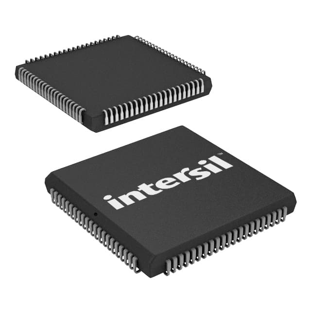
- Part No.:
- HSP45106JC-25Z
- Manufacturer:
- Renesas
- Category:
- Programmable Timers and Oscillators
- Package:
- 84-LCC (J-Lead)
- Datasheet:
-
 HSP45106JC-25Z.pdf
- Description:
- IC OSC NCO 25.6MHZ 84-PLCC
- Quantity:
- Payment:

- Shipping:

Inventory:4,466
Please send an inquiry. Send us your inquiry, and we will respond immediately.
Product details
Overview
HSP45106JC-25Z from Intersil is a 16-bit numerically controlled oscillator (NCO) designed for direct digital synthesis, delivering simultaneous 16-bit quadrature sine and cosine outputs at up to 25.6MHz clock rate, with 32-bit frequency resolution (<0.008Hz at 33MHz), 16-bit phase control (<0.006° resolution), and spurious-free dynamic range >90dBc. It serves as the core waveform generation engine in frequency-hopped modems and precision signal generators.
For engineers reviewing the HSP45106JC-25Z datasheet, HSP45106JC-25Z pinout, HSP45106JC-25Z application, or HSP45106JC-25Z equivalent, key selection considerations include its 84-lead PLCC package, parallel/serial output configurability, two's complement or offset binary encoding, real-time phase/frequency agility, and support for 8-level PSK via discrete MOD(2:0) inputs.
Technical Context
The HSP45106JC-25Z implements a two-stage architecture: a Phase/Frequency Control Section (PFCS) computes a 28-bit instantaneous phase word using 32-bit center/offset frequency adders and a 32-bit phase accumulator, while the Sine/Cosine Section performs 20-bit-addressed ROM lookup to generate 16-bit quadrature outputs. The PFCS accepts microprocessor interface commands (C[15:0], A[2:0], CS, WR) and discrete control signals (ENCFREG, ENOFREG, ENPOREG, MOD[2:0], PMSEL) to update registers synchronously on CLK rising edges.
Output formatting is fully configurable: PAR/SER selects serial (MSB-first on SIN15/COS15, LSB-first on SIN0/COS0) or parallel mode; BINFMT toggles between two's complement and offset binary; OES/OEC enable three-state control of SIN[15:0]/COS[15:0]; and TEST enables phase accumulator readout by multiplexing the 28 MSBs onto the output busses.
Key Specifications
| Parameter | Value and Actual Design Meaning |
|---|---|
| Max Clock Frequency | 25.6MHz - defines maximum sample rate for quadrature output generation and real-time frequency/phase update timing. |
| Frequency Resolution | 32-bit word - enables tuning resolution better than 0.008Hz at 33MHz, critical for narrowband spectral purity in spread spectrum systems. |
| Phase Control Resolution | 16-bit register - provides phase adjustment finer than 0.006°, supporting precise coherent switching and high-order PSK modulation. |
| SFDR | >90dBc - quantifies spurious content suppression in the complex sinusoidal output vector, essential for low-error communication links. |
| Output Format Options | Two's complement or offset binary - ensures compatibility with both signed-input DACs (e.g., HI5731) and unsigned-input converters without external level shifting. |
| Modulation Support | 8-level PSK via MOD[2:0] pins - enables hardware-accelerated phase shifts (0°, 45°, 90°, ..., 315°) without CPU intervention during symbol transitions. |
| Supply Voltage | +4.75V to +5.25V - specifies rail tolerance for stable operation in industrial 5V systems with typical ±5% regulation. |
Pinout & Package
Package: 84-lead plastic leaded chip carrier (PLCC), RoHS-compliant Pb-free finish (e3 termination), JEDEC MO-118AA compliant, thermal resistance θJA = 36°C/W.
| Pin/Terminal | Circuit Role | Design Meaning |
|---|---|---|
| VCC | +5V power supply | Primary logic and analog core supply; requires local 0.1µF decoupling per VCC pin due to high-frequency switching current. |
| GND | Ground reference | Common return for all digital and analog sections; multiple GND pins must be tied to low-impedance ground plane. |
| C[15:0] | 16-bit bidirectional data bus | Loads configuration data into input registers (center/offset frequency, timer, phase) under address decode A[2:0] and WR/CS control. |
| A[2:0] | 3-bit address bus | Selects among seven 16-bit input registers (e.g., A=000 → LSB center frequency; A=110 → phase register). |
| CS, WR | Chip select / write enable | Active-low strobes that latch C[15:0] data into selected input register on WR rising edge when CS is low. |
| CLK | Master system clock input | Drives all internal synchronous logic; rising edge clocks register updates, accumulator increments, and output sampling. |
| ENCFREG, ENOFREG, ENPOREG | Register enable controls | Active-low signals that gate clocked transfer of data from input registers to corresponding 32-bit PFCS control registers. |
| MOD[2:0], PMSEL | PSK modulation interface | Three-pin hardware modulation path: MOD bits set upper 3 bits of phase offset; PMSEL selects between register or MOD source. |
| SIN[15:0], COS[15:0] | Quadrature digital outputs | 16-bit parallel outputs carrying sine/cosine amplitude values; three-stated by OES/OEC; format selectable via BINFMT. |
| PAR/SER, BINFMT | Output configuration | PAR/SER selects parallel (real-time) vs. serial (bit-stream) output mode; BINFMT selects two's complement (signed) or offset binary (unsigned) encoding. |
| OES, OEC | Output enable controls | Active-low enables for SIN[15:0] and COS[15:0] busses; allow shared bus interfacing and power-down of unused outputs. |
| TEST | Diagnostic mode select | When high, routes 28 MSBs of phase accumulator to SIN[15:0]/COS[15:4] for real-time phase monitoring or calibration. |
Key Features
| Feature | Design Value |
|---|---|
| 32-bit frequency control | Enables sub-Hz frequency resolution and phase-coherent switching between two frequencies via independent center/offset registers. |
| Hardware 8-level PSK support | Eliminates software overhead for symbol transitions by mapping MOD[2:0] directly to 45°-incremented phase offsets in real time. |
| Configurable output serialization | Serial mode provides MSB-first (SIN15/COS15) and LSB-first (SIN0/COS0) streams with DACSTRB strobe for DAC synchronization. |
| Test-accessible phase accumulator | TEST pin exposes internal 28-bit phase word for closed-loop calibration, jitter analysis, or debugging without interrupting waveform generation. |
| Pb-free RoHS compliance | e3 matte tin termination supports both SnPb and Pb-free reflow profiles per IPC/JEDEC J-STD-020, with MSL rating matching Pb-free requirements. |
Applications
| Direct Digital Synthesis (DDS) | Spread Spectrum Communications |
|---|---|
Use Scenario: Generating highly stable, programmable RF carriers in test equipment and agile transceivers. IC Role / Device Role / Timing Role: Primary digital waveform synthesizer producing phase- and frequency-agile sine/cosine pairs for IQ upconversion. Use Value: 32-bit frequency resolution enables <0.008Hz step size at 25.6MHz, ensuring minimal spectral leakage in narrowband channelized systems. |
Use Scenario: Implementing frequency-hopping sequences in military comms and secure wireless links. IC Role / Device Role / Timing Role: Real-time NCO core that switches carrier frequency between hops with zero phase discontinuity via center/offset register coordination. Use Value: Phase-coherent switching preserves signal integrity across hops, avoiding transient artifacts that degrade BER in FHSS receivers. |
| PSK Modem Signal Generation | Precision Signal Generation |
Use Scenario: Hardware-accelerated BPSK/QPSK/8PSK modulation in satellite modems and baseband processors. IC Role / Device Role / Timing Role: Direct phase modulator using MOD[2:0] pins to inject discrete phase offsets synchronized to symbol clock. Use Value: Dedicated 3-pin PSK interface reduces FPGA logic resource usage and eliminates CPU latency in symbol timing-critical paths. |
Use Scenario: Calibrating instrumentation-grade ADCs/DACs and generating metrology reference waveforms. IC Role / Device Role / Timing Role: Low-spurious digital source feeding high-resolution DACs (e.g., HI5731) to produce spectrally pure analog test tones. Use Value: >90dBc SFDR ensures harmonic and intermodulation distortion remain below -90dB relative to carrier, meeting Class I calibration standards. |
Equivalent & Alternatives
The following parts are listed as comparable options for similar numerically controlled oscillator applications.
| Alternative Part | Technical Difference | Application Difference | Selection Advice |
|---|---|---|---|
| AD9854ASTZ | Integrated 300MHz DDS with on-chip 12-bit DAC, 48-bit frequency tuning word, and QPSK modulation mode; requires external reconstruction filter. | Higher integration enables single-chip RF synthesis but lacks discrete MOD[2:0] hardware PSK acceleration and 84-lead PLCC footprint. | Choose AD9854ASTZ for higher-frequency RF output and integrated DAC; retain HSP45106JC-25Z for discrete DAC interfacing, PLCC layout compatibility, and dedicated PSK pin control. |
| MAX2748ETL+ | 3.3V CMOS 2.4GHz fractional-N PLL with integrated VCO; no direct digital synthesis capability or quadrature outputs. | Targets RF frequency synthesis rather than baseband waveform generation; unsuitable for DDS, PSK, or quadrature signal applications. | Not functionally equivalent; MAX2748ETL+ serves RF local oscillator roles, whereas HSP45106JC-25Z is a baseband NCO-select only if migrating to PLL-based architectures with different system partitioning. |
Compared with AD9854ASTZ and MAX2748ETL+, the HSP45106JC-25Z offers deterministic 16-bit quadrature outputs with hardware PSK support and PLCC packaging ideal for legacy industrial designs, while AD9854ASTZ provides higher integration at RF frequencies and MAX2748ETL+ addresses entirely different PLL-based frequency synthesis use cases.
Availability
HSP45106JC-25Z is available at Aetrix Electronics and suitable for frequency-hopped modems, precision signal generators, and spread spectrum communications requiring stable component supply and long-term obsolescence management.
Supply support for HSP45106JC-25Z includes scheduled delivery planning, volume procurement assistance, BOM continuity management, traceable sourcing, and lifecycle availability coordination for OEM customers, industrial embedded developers, connected-device designers, and electronics production programs.
Manufacturer
Intersil Corporation was a U.S.-based semiconductor company specializing in high-performance analog and mixed-signal ICs, later acquired by Renesas Electronics in 2017. Its products emphasized precision timing, power management, and RF signal processing.
The HSP45106JC-25Z belongs to Intersil's Numerically Controlled Oscillator (NCO) product line, engineered for applications demanding phase- and frequency-agile digital waveform synthesis-including military comms, test instrumentation, and digital modulation subsystems.
FAQ
What is the maximum operating clock frequency for the HSP45106JC-25Z?
The HSP45106JC-25Z is rated for a maximum clock frequency of 25.6MHz, as indicated by the "-25" suffix in its part number. This defines the upper limit for the CLK input driving the phase accumulator, Sine/Cosine ROM, and all internal synchronous logic. Exceeding this frequency may result in timing violations, metastability, or degraded SFDR performance. The device is not guaranteed to operate reliably at the 33MHz capability documented for the HSP45106JC-33 variant.
How does the HSP45106JC-25Z support 8-level PSK modulation?
The HSP45106JC-25Z supports 8-level PSK through three dedicated input pins-MOD0, MOD1, and MOD2-paired with the PMSEL control. When PMSEL is low, these pins directly encode eight discrete phase offsets (0°, 45°, 90°, 135°, 180°, 225°, 270°, 315°) into the upper 3 bits of the phase offset register, while the lower 13 bits are zeroed. This hardware path enables symbol-rate phase switching without CPU involvement, reducing latency and simplifying modem firmware.
Can the HSP45106JC-25Z output both sine and cosine simultaneously in parallel mode?
Yes, the HSP45106JC-25Z provides simultaneous 16-bit parallel outputs on SIN[15:0] and COS[15:0] pins when PAR/SER is high. Both busses are updated every CLK cycle with new amplitude values derived from the current 28-bit phase argument. Output drive strength and timing meet standard 5V TTL/CMOS levels, and three-state control via OES and OEC allows bus sharing or power-gating of unused channels.
What is the purpose of the TEST pin on the HSP45106JC-25Z?
The TEST pin on the HSP45106JC-25Z enables diagnostic access to the internal 28-bit phase accumulator value. When asserted high (and PAR/SER high), the most significant 28 bits of the phase word are routed to SIN[15:0] and COS[15:4], allowing real-time observation of phase progression without halting waveform generation. This facilitates closed-loop calibration, jitter measurement, and debug of phase-coherent switching behavior in deployed systems.
Is the HSP45106JC-25Z pin-compatible with other variants in the HSP45106 family?
Yes, the HSP45106JC-25Z shares identical 84-lead PLCC pinout and electrical interface with HSP45106JC-25, HSP45106JC-33, and HSP45106JC-33Z. All variants use the same package drawing N84.1.15 and maintain full functional and mechanical compatibility. The "Z" suffix denotes Pb-free RoHS-compliant termination, while the numeric suffix (-25 vs. -33) indicates maximum rated clock frequency-not pinout or register map differences.
HSP45106JC-25Z Specifications
- Product attributes
- Attribute value
- Manufacturer:
- Renesas
- Series:
- -
- Package/Case:
- 84-LCC (J-Lead)
- Packaging:
- Tube
- Product Status:
- Obsolete
- Type:
- Numerically Controlled Oscillator (NCO)
- Count:
- -
- Frequency:
- 25.6MHz
- Voltage - Supply:
- 4.75V ~ 5.25V
- Current - Supply:
- 180 mA
- Operating Temperature:
- 0°C ~ 70°C
- Supplier Device Package:
- 84-PLCC (29.31x29.31)
- Mounting Type:
- Surface Mount
- Grade:
- -
- Qualification:
- -
HSP45106JC-25Z FAQ
1.How can I place an order for HSP45106JC-25Z through Aetrix?
Please submit a Request for Quotation (RFQ) for HSP45106JC-25Z on Aetrix. Our sales agent will provide a competitive quotation and guide you through the order confirmation once you accept the terms.
2.Are the price and stock information for HSP45106JC-25Z reliable?
The price and inventory of HSP45106JC-25Z are updated periodically and may fluctuate due to market conditions. Stock and pricing data are typically refreshed every 24 hours. Quotation validity for HSP45106JC-25Z is usually 5 days.
3.What payment methods are accepted for HSP45106JC-25Z?
We accept Wire Transfer, PayPal, Credit Card, Western Union, MoneyGram, and Escrow for HSP45106JC-25Z transactions.
Note: Certain payment methods may incur a processing fee.
4.How is shipping managed for HSP45106JC-25Z?
HSP45106JC-25Z orders can be shipped via leading logistics carriers, including DHL, UPS, FedEx, TNT, or Registered Mail.
Once your HSP45106JC-25Z order is processed, you will receive an email with the shipment details and tracking number.
Note: Tracking information may take up to 24 hours to appear. Express delivery typically takes 3–5 business days.
5.How can I obtain technical support or documentation for HSP45106JC-25Z?
For technical support, including HSP45106JC-25Z datasheets, pinout diagrams, or application guidance, please contact our engineering support team. They can provide detailed documentation and assistance for your HSP45106JC-25Z requirements.
6.How does Aetrix verify that HSP45106JC-25Z is sourced from the original manufacturer or authorized distributors?
All HSP45106JC-25Z products on Aetrix are procured from qualified distributors and authorized channels. Our dedicated quality assurance team conducts strict verification, including traceability checks and, if necessary, third-party testing. This ensures that HSP45106JC-25Z meets industry standards.
7.What is the process for return or replacement of HSP45106JC-25Z?
All HSP45106JC-25Z units undergo pre-shipment inspection (PSI). If there is an issue with HSP45106JC-25Z, returns or replacements are accepted under the following conditions:
1.Quantity discrepancies, incorrect items, or visible external defects (such as breakage or corrosion), acknowledged by Aetrix.
2.The issue is reported within 90 days of delivery.
3.The HSP45106JC-25Z part is unused and in its original packaging.
Return procedure for HSP45106JC-25Z:
1.Submit a request within 90 days.
2.Obtain a Return Material Authorization (RMA) from Aetrix.
HSP45106JC-25Z Tags

-
NE555DR
Texas Instruments
-
SA555DR
Texas Instruments
-
NA555DR
Texas Instruments
-
SE555DR
Texas Instruments

-
NE555P
Texas Instruments

-
CD4541BM96
Texas Instruments

-
CD4541BE
Texas Instruments
-
TLC555QDR
Texas Instruments
-
TLC555IDR
Texas Instruments
-
TLC555QDRQ1
Texas Instruments

-
TPL5010DDCR
Texas Instruments
-
TLC555CP
Texas Instruments
Tech Hub

A practical engineering and sourcing framework covering lifecycle verification, lifetime-buy calculations, replacement qualification, supplier checks and counterfeit-risk controls.

TTL and CMOS logic families differ in thresholds, loading, output drive, power and timing. This engineering guide compares 74HC and 74HCT, calculates noise margins and checks 3.3 V/5 V compatibility.

A practical engineering guide to 3.3V and 5V logic compatibility, input thresholds, resistor dividers, translator ICs, MOSFET level shifting, I2C pull-ups, timing limits and power-sequencing risks.

The 74HC595 uses push-pull logic outputs, while the TPIC6B595 uses 50 V open-drain DMOS sinks for higher-power loads. This guide compares timing, current limits, 3.3 V interfacing, load wiring, thermal…

The 74HC595 converts serial data into eight stable parallel outputs. This guide covers pin functions, shift and storage timing, OE and MR behavior, drive-current limits, cascading, voltage compatibilit…

A technical comparison of level-sensitive latches and edge-triggered flip-flops, covering timing windows, setup and hold limits, master–slave operation, time borrowing, race-through, HDL inference and…

A D latch stores one bit while Enable controls when data can pass. This reference covers gate-level operation, truth tables, transparency, setup and hold timing, LE versus OE, common ICs and practical …

An SR latch stores one bit through cross-coupled feedback. This engineering reference covers NOR and NAND implementations, truth tables, forbidden-state recovery, gated operation, switch debouncing, fa…

Latch circuits retain one bit through feedback. This technical reference covers SR and D latches, truth tables, transparency, timing limits, latch-versus-flip-flop behavior, applications and common log…

An engineering guide to LED driver operation, constant-current and constant-voltage outputs, linear and switching topologies, dimming, IC selection, calculations, replacement compatibility, and fault c…


