
 My Inquiry
 My Account


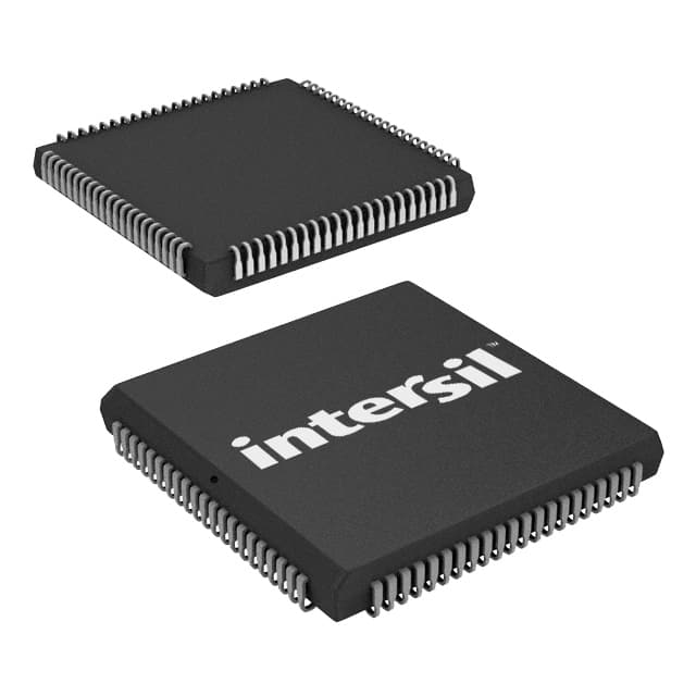
Renesas HSP45106JC-33Z
- Part No.:
- HSP45106JC-33Z
- Manufacturer:
- Renesas
- Category:
- Programmable Timers and Oscillators
- Package:
- 84-LCC (J-Lead)
- Datasheet:
-
 HSP45106JC-33Z.pdf
- Description:
- IC OSC NCO 33MHZ 84-PLCC
- Quantity:
- Payment:

- Shipping:

Inventory:1,458
Please send an inquiry. Send us your inquiry, and we will respond immediately.
Product details
Overview
HSP45106JC-33Z from Intersil is a 16-bit numerically controlled oscillator (NCO) designed for direct digital synthesis and quadrature signal generation in frequency-agile communication systems. It delivers simultaneous 16-bit sine and cosine outputs at up to 33MHz clock rate, with 32-bit frequency resolution (<0.008Hz at 33MHz), 16-bit phase control (<0.006° resolution), and >90dBc spurious-free dynamic range. It supports 8-level PSK modulation via discrete MOD(2:0) inputs and operates across 0°C to +70°C.
For engineers reviewing the HSP45106JC-33Z datasheet, HSP45106JC-33Z pinout, HSP45106JC-33Z application, or HSP45106JC-33Z equivalent, key selection criteria include its 84-lead PLCC package, parallel/serial output flexibility, two's complement or offset binary encoding, real-time phase/frequency agility, and compatibility with DAC interfaces in spread spectrum, PSK modem, and precision signal generation designs.
Technical Context
The HSP45106JC-33Z implements a two-stage architecture: a Phase/Frequency Control Section (PFCS) generating a 28-bit instantaneous phase word from 32-bit center/offset frequency and 16-bit phase offset registers, followed by a Sine/Cosine Section performing 20-bit-address ROM lookup to produce 16-bit quadrature outputs. Its PFCS includes a 32-bit phase accumulator, timer accumulator with TICO carry output, and discrete modulation logic synchronized to CLK.
Control is executed via an 16-bit microprocessor bus (C[15:0]) with A[2:0] address decoding, active-low CS/WR, and dedicated enable lines (ENCFREG, ENOFREG, ENPOREG, ENPHAC) that register on CLK rising edges. Output format (two's complement/offset binary) and interface mode (parallel/serial) are selected dynamically via BINFMT and PAR/SER pins, both registered on CLK.
Key Specifications
| Parameter | Value and Actual Design Meaning |
|---|---|
| Max Clock Frequency | 33MHz - determines maximum sample rate for quadrature output generation and real-time frequency/phase update speed. |
| Frequency Resolution | 32-bit word - enables <0.008Hz tuning step at 33MHz, critical for narrowband frequency-hopping and precise DDS applications. |
| Phase Resolution | 16-bit control - provides <0.006° phase step resolution, supporting high-fidelity 8PSK and coherent phase switching. |
| Output Format Options | Two's complement or offset binary - simplifies direct interfacing with common DACs without external level-shifting circuitry. |
| SFDR | >90dBc - ensures minimal spectral contamination in sensitive RF and communications signal chains. |
| Output Interface | Parallel (SIN/COS[15:0]) or serial (MSB-first on SIN15/COS15, LSB-first on SIN0/COS0) - offers layout and timing flexibility for system integration. |
| Supply Voltage | +4.75V to +5.25V - compatible with standard 5V logic and mixed-signal systems requiring tight regulation. |
Pinout & Package
Package: 84-lead Plastic Leaded Chip Carrier (PLCC), RoHS-compliant Pb-free finish (e3 termination), 0°C to +70°C operating range.
| Pin/Terminal | Circuit Role | Design Meaning |
|---|---|---|
| VCC | +5V power supply | Primary power rail for all internal logic and analog sections; requires local decoupling per high-speed NCO operation. |
| GND | Ground reference | Digital and analog ground return; multiple GND pins support low-impedance return paths for noise-sensitive quadrature outputs. |
| C[15:0] | 16-bit bidirectional control data bus | Loads configuration data into input registers (center/offset frequency, phase, timer); LSB-aligned (C0 = LSB). |
| A[2:0] | Address select for C[15:0] destination | Selects among seven 16-bit input registers (e.g., A[2:0]=000 → LSB Center Freq); decoded per Table 1 in datasheet. |
| CS, WR | Chip select and write enable | Active-low synchronous interface controls register loading; WR rising edge clocks data when CS is low. |
| CLK | Main system clock input | Drives all internal registers and accumulators; rising edge synchronizes ENxREG signals and updates PFCS state. |
| ENCFREG / ENOFREG / ENPOREG / ENPHAC | Register enable controls | Active-low, CLK-registered enables for downloading data from input registers to PFCS control registers (e.g., ENCFREG → Center Freq Register). |
| MOD[2:0], PMSEL | 8PSK modulation interface | Three-pin discrete interface for 0°–315° phase shifts; PMSEL selects between register-loaded or MOD-driven phase offset. |
| PAR/SER, BINFMT | Output configuration | CLK-registered mode selects: PAR/SER = high → parallel output; BINFMT = low → two's complement, high → offset binary. |
| OES, OEC | Output enable for sine/cosine buses | Active-low three-state control; allows shared bus usage or output disabling during configuration sequences. |
| SIN[15:0], COS[15:0] | 16-bit quadrature digital outputs | Simultaneous sine/cosine amplitude values; in serial mode, SIN15/COS15 = MSB-first, SIN0/COS0 = LSB-first streams. |
| DACSTRB | DAC strobe output | Active-low pulse indicating first bit of new serial word is valid; essential for synchronizing external DAC sampling in serial mode. |
Key Features
| Feature | Design Value |
|---|---|
| 32-bit frequency control | Enables sub-Hz frequency agility at 33MHz clock, supporting precise channel spacing in frequency-hopped spread spectrum systems. |
| 16-bit phase control with MOD[2:0] interface | Allows real-time 8PSK modulation without processor intervention-critical for low-latency BPSK/QPSK/8PSK modem implementations. |
| Configurable output encoding and interface | Eliminates need for external format conversion logic when interfacing with TI, ADI, or Maxim DACs supporting either two's complement or offset binary inputs. |
| Test mode with phase accumulator readout | Permits verification of internal phase state via SIN/COS pins while bypassing ROM lookup-valuable for calibration and debug of DDS loop stability. |
| Timer accumulator with TICO output | Generates programmable periodic interrupts (e.g., for frame sync or DAC update triggers) independent of main NCO output timing. |
Applications
| Direct Digital Synthesis (DDS) | Spread Spectrum Communications |
|---|---|
Use Scenario: Generating stable, tunable RF carrier waveforms in software-defined radio transceivers where frequency must be updated in microseconds. IC Role / Device Role / Timing Role: Primary quadrature waveform generator; produces synchronized 16-bit sine/cosine samples at 33MHz for IQ modulation. Use Value: 32-bit frequency resolution enables <0.008Hz step size, allowing precise channel selection and fine-grained frequency synthesis without analog VCO drift. |
Use Scenario: Implementing frequency-hopping sequences in military-grade secure comms where hop timing and phase coherence between hops are mandatory. IC Role / Device Role / Timing Role: NCO core providing phase-coherent switching between two programmed frequencies using INHOFR and dual frequency registers. Use Value: Preserves register contents during hop transitions and maintains phase continuity-reducing spectral splatter and improving BER in FHSS links. |
| PSK Modem Systems | Precision Signal Generation |
Use Scenario: Real-time BPSK/QPSK/8PSK modulation in satellite telemetry modems where low-latency symbol mapping is required. IC Role / Device Role / Timing Role: Quadrature signal source with hardware-accelerated phase modulation via MOD[2:0] pins and PMSEL control. Use Value: Eliminates CPU overhead for symbol mapping; discrete 3-pin interface achieves <100ns phase switch time, meeting stringent modem timing budgets. |
Use Scenario: Calibrating high-resolution ADCs/DACs in metrology equipment requiring ultra-low-jitter, spectrally pure test tones. IC Role / Device Role / Timing Role: Reference waveform generator delivering >90dBc SFDR quadrature outputs for stimulus generation. Use Value: Spurious components <-90dBc ensure measurement accuracy unaffected by harmonic distortion, enabling <16-bit effective resolution in test setups. |
Equivalent & Alternatives
The following parts are listed as comparable options for similar numerically controlled oscillator applications.
| Alternative Part | Technical Difference | Application Difference | Selection Advice |
|---|---|---|---|
| AD9854ASTZ | Integrated 300MHz DDS with on-chip 12-bit DAC, 48-bit frequency tuning, and SPI interface; requires external reconstruction filter. | Better suited for wideband RF synthesis (>100MHz) but lacks discrete 8PSK modulation pins and PLCC packaging. | Choose AD9854ASTZ when higher output frequency, integrated DAC, or SPI simplicity outweighs need for hardware PSK modulation and legacy PLCC footprint. |
| MAX2748ETL+ | 3.3V CMOS NCO with 24-bit tuning, 16-bit outputs, and I²C interface; smaller 40-pin TQFN package, no MOD[2:0] pins. | Targets battery-powered portable radios; lacks phase accumulator readout mode and timer accumulator with TICO output. | Choose MAX2748ETL+ for space-constrained, low-power designs where 3.3V operation and I²C control are prioritized over 5V compatibility and advanced timing features. |
Compared with AD9854ASTZ and MAX2748ETL+, the HSP45106JC-33Z uniquely combines 5V operation, 84-pin PLCC packaging, dedicated hardware PSK modulation pins, phase accumulator visibility, and timer-based interrupt generation-making it optimal for legacy industrial and defense systems requiring field-upgradeable, deterministic NCO behavior.
Availability
HSP45106JC-33Z is available at Aetrix Electronics and suitable for frequency-hopped modems, PSK modems, and precision signal generators requiring stable component supply across extended production lifecycles.
Supply support for HSP45106JC-33Z includes scheduled delivery planning, volume procurement assistance, BOM continuity management, traceable sourcing, and lifecycle availability coordination for OEM customers, industrial embedded developers, connected-device designers, and electronics production programs.
Manufacturer
Intersil Corporation was a U.S.-based semiconductor company specializing in high-performance analog and mixed-signal ICs, later acquired by Renesas Electronics in 2017.
The HSP45106JC-33Z belongs to Intersil's high-precision numerically controlled oscillator product line, engineered for demanding communications infrastructure and test equipment requiring deterministic phase/frequency agility and quadrature signal integrity.
FAQ
What is the maximum operating clock frequency supported by the HSP45106JC-33Z?
The HSP45106JC-33Z is rated for a maximum clock frequency of 33MHz, as indicated by the "-33" suffix in its part number. This defines the upper limit for both the internal phase accumulator update rate and the sample rate of its 16-bit sine and cosine outputs. Operation above this frequency is not guaranteed and may result in timing violations or degraded SFDR performance.
Does the HSP45106JC-33Z support both parallel and serial output modes?
Yes, the HSP45106JC-33Z supports both parallel and serial output configurations. The PAR/SER pin selects the mode: when high, 16-bit sine and cosine data appear simultaneously on SIN[15:0] and COS[15:0]; when low, data is shifted out serially with MSB-first on SIN15/COS15 and LSB-first on SIN0/COS0, synchronized by DACSTRB.
How does the HSP45106JC-33Z implement 8-level PSK modulation?
The HSP45106JC-33Z implements 8-level PSK using three discrete MOD[2:0] inputs and the PMSEL pin. When PMSEL is low, MOD[2:0] directly set the three most significant bits of the phase offset register, producing eight distinct phase shifts (0°, 45°, 90°, 135°, 180°, 225°, 270°, 315°), while the lower 13 bits are zeroed-enabling hardware-accelerated symbol mapping without processor involvement.
What is the purpose of the TEST pin on the HSP45106JC-33Z?
The TEST pin on the HSP45106JC-33Z enables diagnostic access to the internal 28-bit phase accumulator output. When asserted high (with PAR/SER also high), the most significant bits of the phase accumulator are routed to SIN[15:0] and COS[15:4], bypassing the Sine/Cosine ROM lookup. This allows real-time verification of phase progression during system bring-up or calibration.
Is the HSP45106JC-33Z RoHS compliant?
Yes, the HSP45106JC-33Z is RoHS compliant. The "Z" suffix denotes Intersil's Pb-free plastic packaging, featuring 100% matte tin (e3) termination finish, compatible with both SnPb and lead-free soldering processes, and meeting IPC/JEDEC J-STD-020 reflow requirements.
HSP45106JC-33Z Specifications
- Product attributes
- Attribute value
- Manufacturer:
- Renesas
- Series:
- -
- Package/Case:
- 84-LCC (J-Lead)
- Packaging:
- Tube
- Product Status:
- Obsolete
- Type:
- Numerically Controlled Oscillator (NCO)
- Count:
- -
- Frequency:
- 33MHz
- Voltage - Supply:
- 4.75V ~ 5.25V
- Current - Supply:
- 180 mA
- Operating Temperature:
- 0°C ~ 70°C
- Supplier Device Package:
- 84-PLCC (29.31x29.31)
- Mounting Type:
- Surface Mount
- Grade:
- -
- Qualification:
- -
HSP45106JC-33Z FAQ
1.How can I place an order for HSP45106JC-33Z through Aetrix?
Please submit a Request for Quotation (RFQ) for HSP45106JC-33Z on Aetrix. Our sales agent will provide a competitive quotation and guide you through the order confirmation once you accept the terms.
2.Are the price and stock information for HSP45106JC-33Z reliable?
The price and inventory of HSP45106JC-33Z are updated periodically and may fluctuate due to market conditions. Stock and pricing data are typically refreshed every 24 hours. Quotation validity for HSP45106JC-33Z is usually 5 days.
3.What payment methods are accepted for HSP45106JC-33Z?
We accept Wire Transfer, PayPal, Credit Card, Western Union, MoneyGram, and Escrow for HSP45106JC-33Z transactions.
Note: Certain payment methods may incur a processing fee.
4.How is shipping managed for HSP45106JC-33Z?
HSP45106JC-33Z orders can be shipped via leading logistics carriers, including DHL, UPS, FedEx, TNT, or Registered Mail.
Once your HSP45106JC-33Z order is processed, you will receive an email with the shipment details and tracking number.
Note: Tracking information may take up to 24 hours to appear. Express delivery typically takes 3–5 business days.
5.How can I obtain technical support or documentation for HSP45106JC-33Z?
For technical support, including HSP45106JC-33Z datasheets, pinout diagrams, or application guidance, please contact our engineering support team. They can provide detailed documentation and assistance for your HSP45106JC-33Z requirements.
6.How does Aetrix verify that HSP45106JC-33Z is sourced from the original manufacturer or authorized distributors?
All HSP45106JC-33Z products on Aetrix are procured from qualified distributors and authorized channels. Our dedicated quality assurance team conducts strict verification, including traceability checks and, if necessary, third-party testing. This ensures that HSP45106JC-33Z meets industry standards.
7.What is the process for return or replacement of HSP45106JC-33Z?
All HSP45106JC-33Z units undergo pre-shipment inspection (PSI). If there is an issue with HSP45106JC-33Z, returns or replacements are accepted under the following conditions:
1.Quantity discrepancies, incorrect items, or visible external defects (such as breakage or corrosion), acknowledged by Aetrix.
2.The issue is reported within 90 days of delivery.
3.The HSP45106JC-33Z part is unused and in its original packaging.
Return procedure for HSP45106JC-33Z:
1.Submit a request within 90 days.
2.Obtain a Return Material Authorization (RMA) from Aetrix.
HSP45106JC-33Z Tags

-
NE555DR
Texas Instruments
-
SA555DR
Texas Instruments
-
NA555DR
Texas Instruments
-
SE555DR
Texas Instruments

-
NE555P
Texas Instruments

-
CD4541BM96
Texas Instruments

-
CD4541BE
Texas Instruments
-
TLC555QDR
Texas Instruments
-
TLC555IDR
Texas Instruments
-
TLC555QDRQ1
Texas Instruments

-
TPL5010DDCR
Texas Instruments
-
TLC555CP
Texas Instruments
Tech Hub

A practical engineering and sourcing framework covering lifecycle verification, lifetime-buy calculations, replacement qualification, supplier checks and counterfeit-risk controls.

TTL and CMOS logic families differ in thresholds, loading, output drive, power and timing. This engineering guide compares 74HC and 74HCT, calculates noise margins and checks 3.3 V/5 V compatibility.

A practical engineering guide to 3.3V and 5V logic compatibility, input thresholds, resistor dividers, translator ICs, MOSFET level shifting, I2C pull-ups, timing limits and power-sequencing risks.

The 74HC595 uses push-pull logic outputs, while the TPIC6B595 uses 50 V open-drain DMOS sinks for higher-power loads. This guide compares timing, current limits, 3.3 V interfacing, load wiring, thermal…

The 74HC595 converts serial data into eight stable parallel outputs. This guide covers pin functions, shift and storage timing, OE and MR behavior, drive-current limits, cascading, voltage compatibilit…

A technical comparison of level-sensitive latches and edge-triggered flip-flops, covering timing windows, setup and hold limits, master–slave operation, time borrowing, race-through, HDL inference and…

A D latch stores one bit while Enable controls when data can pass. This reference covers gate-level operation, truth tables, transparency, setup and hold timing, LE versus OE, common ICs and practical …

An SR latch stores one bit through cross-coupled feedback. This engineering reference covers NOR and NAND implementations, truth tables, forbidden-state recovery, gated operation, switch debouncing, fa…

Latch circuits retain one bit through feedback. This technical reference covers SR and D latches, truth tables, transparency, timing limits, latch-versus-flip-flop behavior, applications and common log…

An engineering guide to LED driver operation, constant-current and constant-voltage outputs, linear and switching topologies, dimming, IC selection, calculations, replacement compatibility, and fault c…


