
 My Inquiry
 My Account


Renesas HSP45116AVC-52Z
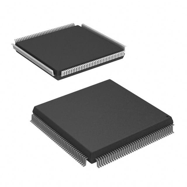
- Part No.:
- HSP45116AVC-52Z
- Manufacturer:
- Renesas
- Category:
- Programmable Timers and Oscillators
- Package:
- 160-BQFP
- Datasheet:
-
 HSP45116AVC-52Z.pdf
- Description:
- IC OSC NCO 52MHZ 160-MQFP
- Quantity:
- Payment:

- Shipping:

Inventory:2,684
Please send an inquiry. Send us your inquiry, and we will respond immediately.
Product details
Overview
HSP45116AVC-52Z from Intersil is a 52MHz numerically controlled oscillator/modulator IC integrating a 32-bit phase/frequency control section, 16-bit quadrature sine/cosine generator, and 16-bit complex multiplier/accumulator (CMAC) in a single monolithic CMOS device. It delivers >90dBc spurious-free dynamic range, programmable 20-bit output resolution, and supports real-time quadrature modulation/demodulation for RF signal processing at up to 40MHz sample rate.
For engineers reviewing the HSP45116AVC-52Z datasheet, HSP45116AVC-52Z pinout, HSP45116AVC-52Z application, or HSP45116AVC-52Z equivalent, this device serves as a high-precision digital frequency synthesis and complex vector modulation engine - particularly relevant for direct digital synthesis (DDS), QAM/PSK modulators, PLL-based receivers, and FFT butterfly computation in communications infrastructure.
Technical Context
The HSP45116AVC-52Z implements a fully static CMOS architecture with three synchronized functional blocks: a 32-bit phase accumulator generating the sine/cosine argument, a 20-bit address ROM lookup producing 16-bit two's complement sin/cos outputs, and a 33-bit complex multiplier feeding dual 20-bit accumulators. Its phase resolution enables 0.013Hz tuning step at 52MHz clock.
Control is executed via parallel microprocessor interface (C0–C15, AD0/AD1, CS, WR) and dedicated logic lines (ENPHREG, ENCFREG, MODPI/2PI, ACC, BINFMT), supporting both CW synthesis and dynamic FM/PSK/FSK modulation. Output multiplexing (OUTMUX0/1), rounding (RND), and block floating-point growth detection (DET0/DET1) are hardware-configurable without firmware overhead.
Key Specifications
| Parameter | Value and Actual Design Meaning |
|---|---|
| Core Function | Numerically Controlled Oscillator + Complex Multiplier/Accumulator (NCO/CMAC) for quadrature modulation/demodulation |
| Max Clock Frequency | 52MHz - defines maximum sample rate and phase update timing for real-time signal generation |
| Phase Resolution | 32 bits - enables frequency tuning resolution better than 0.013Hz at 52MHz |
| SFDR | >90dBc - ensures spectral purity critical for high-order QAM and low-error-rate demodulation |
| Output Word Width | 20-bit programmable (RO0–RO19, IO0–IO19) - supports precision scaling for DAC interfacing or cascaded FFT stages |
| Input Data Format | Two's complement RIN0–RIN18 / IMIN0–IMIN18 - aligns with standard DSP data paths and signed arithmetic |
| Modulation Support | AM, FM, PSK, FSK, QAM, polar-to-Cartesian conversion - enabled by real-time phase/frequency/phase-offset control |
Pinout & Package
160-lead MQFP (28mm × 28mm), Pb-free RoHS-compliant package (Q160.28x28 drawing). Fully static CMOS operation at +5V supply.
| Pin/Terminal | Circuit Role | Design Meaning |
|---|---|---|
| C0–C15 | Parallel control bus | Loads 16-bit segments into phase/frequency/time registers; C15 = MSB |
| AD0, AD1 | Address select | Decodes C0–C15 destination: LS/MS frequency, phase register, or reserved (Table 1) |
| CLK | Master timing reference | Rising-edge clock synchronizes all internal registers and accumulators |
| ENCFREG, ENOFREG, ENPHREG | Register enable controls | Active-low signals that gate clocked loading of center/offset/phase registers |
| RO0–RO19, IO0–IO19 | Programmable output buses | Three-state, multiplexed outputs delivering CMAC or accumulator results in 2's complement or offset binary |
| MOD0, MOD1, PMSEL | External phase modulation interface | Selects 0°/90°/180°/270° phase offsets for QPSK; bypasses full phase register when PMSEL = low |
| ACC, RND, BINFMT | Functional configuration | ACC enables accumulation/dump mode; RND activates output rounding; BINFMT selects 2's complement vs. unsigned output format |
Key Features
| Feature | Design Value |
|---|---|
| Integrated NCO + CMAC | Eliminates inter-chip timing skew and board-level routing complexity in quadrature signal chains |
| 32-bit phase accumulator | Enables sub-Hz frequency resolution and ultra-stable carrier synthesis at 52MHz clock |
| Programmable output multiplexing (OUTMUX0/1) | Routes CMAC 31–34/15–30 or accumulator 0–19 outputs to RO/IO pins without external logic |
| Block floating-point growth detection (DET0/DET1) | Automatically monitors bit growth across CMAC and accumulator holding registers to prevent overflow in cascaded FFTs |
| ROM bypass (RBYTILD) | Directs raw 16-bit phase adder output to CMAC inputs - essential for twiddle factor generation in FFT butterfly engines |
| Pb-free + anneal process | RoHS-compliant 100% matte tin termination compatible with SnPb and Pb-free reflow profiles per IPC/JEDEC J-STD-020 |
Applications
| Direct Digital Synthesis (DDS) | Quadrature Modulator for QAM/PSK |
|---|---|
Use Scenario: Generating stable, agile RF carriers in software-defined radio transmitters with fine frequency resolution and low phase noise. IC Role / Device Role / Timing Role: Acts as the core digital waveform synthesizer, accepting frequency/phase words and outputting synchronized 16-bit sin/cos vectors at 52MHz clock rate. Use Value: Replaces analog VCO/PLL combinations with digitally programmable, temperature-stable, and jitter-immune frequency sources. |
Use Scenario: Implementing 16-QAM or π/4-DQPSK modulation in baseband processors for wireless infrastructure equipment. IC Role / Device Role / Timing Role: Performs real-time complex multiplication of baseband I/Q data with internally generated carrier vectors, supporting dynamic symbol rate changes. Use Value: Delivers >90dBc SFDR and programmable output bit-width to meet EVM and ACLR requirements in multi-carrier systems. |
| Quadrature Downconverter | FFT Butterfly Engine |
Use Scenario: Converting IF signals to baseband in zero-IF receivers for satellite communications and radar front-ends. IC Role / Device Role / Timing Role: Functions as a digital mixer: external IF samples enter via RIN/IMIN, while the NCO generates rotating (cos,sin) vectors for synchronous downconversion. Use Value: Enables precise center-frequency tuning and eliminates image-rejection filter requirements through digital quadrature balance. |
Use Scenario: Accelerating radix-2 decimation-in-frequency FFT computation in spectrum analyzers and channelizers. IC Role / Device Role / Timing Role: Computes one FFT butterfly per clock cycle using ROM-bypassed phase output and shift-controlled inputs for twiddle factor application. Use Value: Reduces FPGA/DSP resource usage by offloading complex multiply-accumulate and bit-growth monitoring to dedicated silicon. |
Equivalent & Alternatives
The following parts are listed as comparable options for similar numerically controlled oscillator/modulator applications.
| Alternative Part | Technical Difference | Application Difference | Selection Advice |
|---|---|---|---|
| AD9858ASTZ | Integrated 10-bit DAC, 1GSPS system clock, no on-chip CMAC; higher integration but lower precision and no complex accumulation | Better suited for wideband analog output applications; lacks hardware FFT support and programmable accumulation | Choose AD9858ASTZ when analog output and ultra-high speed (>100MHz) are required over digital signal processing flexibility |
| MAX2190ETM+ | RF front-end IC with integrated mixer, LNA, and IF amplifier; no NCO or digital modulation capability | Designed for receive-path signal conditioning only; requires external digital modulator for transmit functions | Choose MAX2190ETM+ only for analog IF receiver chain integration - not a functional alternative for digital NCO/CMAC tasks |
Compared with AD9858ASTZ and MAX2190ETM+, the HSP45116AVC-52Z uniquely combines high-resolution NCO synthesis with hardware-accelerated complex multiplication and accumulation - making it irreplaceable for digital-domain quadrature processing where bit-true reproducibility, programmable output formatting, and FFT-ready growth detection are mandatory.
Availability
HSP45116AVC-52Z is available at Aetrix Electronics and suitable for RF signal processing, digital communications infrastructure, and test & measurement equipment requiring stable component supply and long-term obsolescence management.
Supply support for HSP45116AVC-52Z includes scheduled delivery planning, volume procurement assistance, BOM continuity management, traceable sourcing, and lifecycle availability coordination for OEM customers, industrial embedded developers, connected-device designers, and electronics production programs.
Manufacturer
Intersil (now part of Renesas Electronics) is a semiconductor company specializing in high-performance analog and mixed-signal ICs for power management, precision analog, and RF signal processing.
The HSP45116A product line was designed specifically for digital quadrature modulation, direct digital synthesis, and FFT acceleration in communications and instrumentation - targeting engineers needing deterministic, hardware-based complex arithmetic without FPGA overhead.
FAQ
What is the primary function of the HSP45116AVC-52Z?
The HSP45116AVC-52Z is a numerically controlled oscillator/modulator IC combining a 32-bit NCO and a 16-bit complex multiplier/accumulator. Its primary function is to generate high-purity quadrature sinusoids and perform real-time complex multiplication for modulation, demodulation, and FFT computation. The HSP45116AVC-52Z operates at up to 52MHz and delivers >90dBc spurious-free dynamic range, making it suitable for demanding RF and digital signal processing applications.
Does the HSP45116AVC-52Z support QPSK modulation?
Yes, the HSP45116AVC-52Z supports QPSK modulation via its external phase modulation interface (MOD0/MOD1 and PMSEL pins). When PMSEL is low, MOD0 and MOD1 directly load 2-bit phase offsets (0°, 90°, 180°, or 270°) into the most significant bits of the phase register, enabling hardware-accelerated QPSK symbol mapping without CPU intervention. This functionality is explicitly documented in Table 2 of the FN4156 datasheet for the HSP45116AVC-52Z.
What is the purpose of the RBYTILD pin on the HSP45116AVC-52Z?
The RBYTILD (ROM Bypass / Timer Load) pin on the HSP45116AVC-52Z, when asserted low, bypasses the sine/cosine ROM lookup and routes the raw 16-bit phase adder output and lower 16 bits of the phase accumulator directly to the CMAC's sine and cosine inputs. This mode is essential for FFT butterfly computation, where the NCO output serves as twiddle factors rather than sinusoidal waveforms. The HSP45116AVC-52Z uses this feature to enable high-speed, deterministic FFT acceleration without external memory or control logic.
How does the HSP45116AVC-52Z handle output data formatting?
The HSP45116AVC-52Z provides flexible output formatting via the BINFMT pin and OUTMUX0/OUTMUX1 control lines. BINFMT selects between two's complement (default) and offset binary (unsigned) output formats by inverting RO19 and IO19 when low - critical for interfacing with DACs requiring unsigned input. OUTMUX0/1 selects among four output sources: CMAC high/low bits, accumulator outputs, or reserved states (Table 4). This allows the HSP45116AVC-52Z to adapt its 20-bit outputs to varying downstream data path requirements without external glue logic.
Is the HSP45116AVC-52Z still recommended for new designs?
No, the HSP45116AVC-52Z is marked "NOT RECOMMENDED FOR NEW DESIGNS" in the official Intersil FN4156 datasheet (Rev 4.00, May 2007), with no recommended replacement provided. While fully functional and supported for legacy program continuity, new designs should evaluate modern alternatives such as the AD9910 or integrated RF SoCs offering higher integration, lower power, and extended lifecycle. Aetrix Electronics maintains inventory and supply chain support for the HSP45116AVC-52Z to serve existing production and repair needs.
HSP45116AVC-52Z Specifications
- Product attributes
- Attribute value
- Manufacturer:
- Renesas
- Series:
- -
- Package/Case:
- 160-BQFP
- Packaging:
- Tray
- Product Status:
- Obsolete
- Type:
- Numerically Controlled Oscillator (NCO)
- Count:
- -
- Frequency:
- 52MHz
- Voltage - Supply:
- 4.75V ~ 5.25V
- Current - Supply:
- 184 mA
- Operating Temperature:
- 0°C ~ 70°C
- Supplier Device Package:
- 160-MQFP (28x28)
- Mounting Type:
- Surface Mount
- Grade:
- -
- Qualification:
- -
HSP45116AVC-52Z FAQ
1.How can I place an order for HSP45116AVC-52Z through Aetrix?
Please submit a Request for Quotation (RFQ) for HSP45116AVC-52Z on Aetrix. Our sales agent will provide a competitive quotation and guide you through the order confirmation once you accept the terms.
2.Are the price and stock information for HSP45116AVC-52Z reliable?
The price and inventory of HSP45116AVC-52Z are updated periodically and may fluctuate due to market conditions. Stock and pricing data are typically refreshed every 24 hours. Quotation validity for HSP45116AVC-52Z is usually 5 days.
3.What payment methods are accepted for HSP45116AVC-52Z?
We accept Wire Transfer, PayPal, Credit Card, Western Union, MoneyGram, and Escrow for HSP45116AVC-52Z transactions.
Note: Certain payment methods may incur a processing fee.
4.How is shipping managed for HSP45116AVC-52Z?
HSP45116AVC-52Z orders can be shipped via leading logistics carriers, including DHL, UPS, FedEx, TNT, or Registered Mail.
Once your HSP45116AVC-52Z order is processed, you will receive an email with the shipment details and tracking number.
Note: Tracking information may take up to 24 hours to appear. Express delivery typically takes 3–5 business days.
5.How can I obtain technical support or documentation for HSP45116AVC-52Z?
For technical support, including HSP45116AVC-52Z datasheets, pinout diagrams, or application guidance, please contact our engineering support team. They can provide detailed documentation and assistance for your HSP45116AVC-52Z requirements.
6.How does Aetrix verify that HSP45116AVC-52Z is sourced from the original manufacturer or authorized distributors?
All HSP45116AVC-52Z products on Aetrix are procured from qualified distributors and authorized channels. Our dedicated quality assurance team conducts strict verification, including traceability checks and, if necessary, third-party testing. This ensures that HSP45116AVC-52Z meets industry standards.
7.What is the process for return or replacement of HSP45116AVC-52Z?
All HSP45116AVC-52Z units undergo pre-shipment inspection (PSI). If there is an issue with HSP45116AVC-52Z, returns or replacements are accepted under the following conditions:
1.Quantity discrepancies, incorrect items, or visible external defects (such as breakage or corrosion), acknowledged by Aetrix.
2.The issue is reported within 90 days of delivery.
3.The HSP45116AVC-52Z part is unused and in its original packaging.
Return procedure for HSP45116AVC-52Z:
1.Submit a request within 90 days.
2.Obtain a Return Material Authorization (RMA) from Aetrix.
HSP45116AVC-52Z Tags

-
NE555DR
Texas Instruments
-
SA555DR
Texas Instruments
-
NA555DR
Texas Instruments
-
SE555DR
Texas Instruments

-
NE555P
Texas Instruments

-
CD4541BM96
Texas Instruments

-
CD4541BE
Texas Instruments
-
TLC555QDR
Texas Instruments
-
TLC555IDR
Texas Instruments
-
TLC555QDRQ1
Texas Instruments

-
TPL5010DDCR
Texas Instruments
-
TLC555CP
Texas Instruments
Tech Hub

TTL and CMOS logic families differ in thresholds, loading, output drive, power and timing. This engineering guide compares 74HC and 74HCT, calculates noise margins and checks 3.3 V/5 V compatibility.

A practical engineering guide to 3.3V and 5V logic compatibility, input thresholds, resistor dividers, translator ICs, MOSFET level shifting, I2C pull-ups, timing limits and power-sequencing risks.

The 74HC595 uses push-pull logic outputs, while the TPIC6B595 uses 50 V open-drain DMOS sinks for higher-power loads. This guide compares timing, current limits, 3.3 V interfacing, load wiring, thermal…

The 74HC595 converts serial data into eight stable parallel outputs. This guide covers pin functions, shift and storage timing, OE and MR behavior, drive-current limits, cascading, voltage compatibilit…

A technical comparison of level-sensitive latches and edge-triggered flip-flops, covering timing windows, setup and hold limits, master–slave operation, time borrowing, race-through, HDL inference and…

A D latch stores one bit while Enable controls when data can pass. This reference covers gate-level operation, truth tables, transparency, setup and hold timing, LE versus OE, common ICs and practical …

An SR latch stores one bit through cross-coupled feedback. This engineering reference covers NOR and NAND implementations, truth tables, forbidden-state recovery, gated operation, switch debouncing, fa…

Latch circuits retain one bit through feedback. This technical reference covers SR and D latches, truth tables, transparency, timing limits, latch-versus-flip-flop behavior, applications and common log…

An engineering guide to LED driver operation, constant-current and constant-voltage outputs, linear and switching topologies, dimming, IC selection, calculations, replacement compatibility, and fault c…

Operational amplifier guide covering op amp basics, feedback, ideal vs real op amps, common configurations, buffer circuits, offset, bias current, gain-bandwidth, slew rate, rail-to-rail limits and sel…


