
 My Inquiry
 My Account


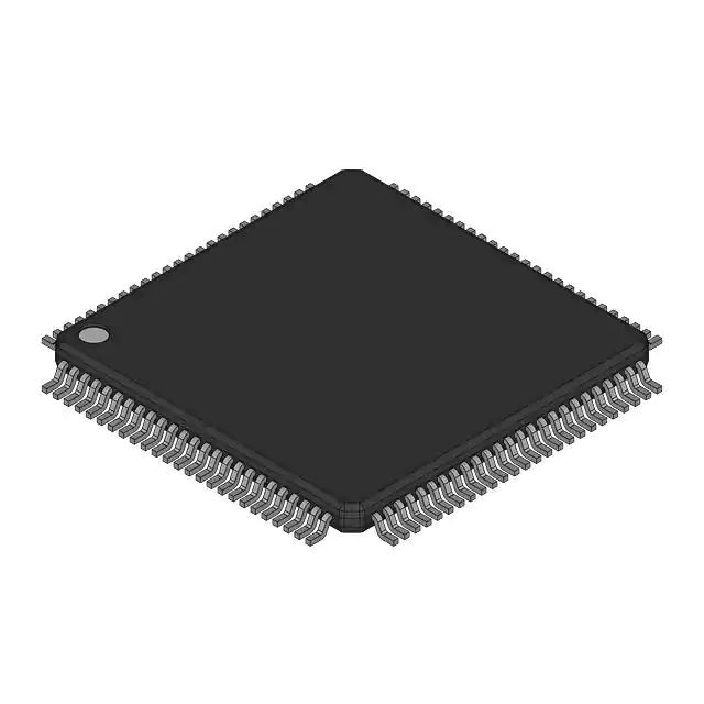
Renesas HSP50415VI
- Part No.:
- HSP50415VI
- Manufacturer:
- Renesas
- Category:
- RF Modulators
- Package:
- -
- Datasheet:
-
 HSP50415VI.pdf
- Description:
- IC MODULATOR PROGRAMABLE 100MQFP
- Quantity:
- Payment:

- Shipping:

Inventory:2,191
Please send an inquiry. Send us your inquiry, and we will respond immediately.
Product details
Overview
HSP50415VI from Intersil is a wideband programmable quadrature amplitude modulator (QAM/PM upconverter) integrating shaping FIR filters, dual 12-bit DACs, carrier and symbol NCOs, and digital PLL timing recovery. It accepts up to 16-bit I/Q data at ≤25MSPS, outputs 14-bit digital or 12-bit analog IF signals at up to 100MSPS, and delivers >70dB SFDR in digital domain and >50dB SFDR through DACs - deployed in base station RF front-ends for 3G/4G wireless infrastructure.
For engineers reviewing the HSP50415VI datasheet, HSP50415VI pinout, HSP50415VI application, or HSP50415VI equivalent, key selection considerations include its 32-bit carrier NCO tuning range (0.023Hz–50MHz), X/SIN(X) rolloff compensation, programmable 24-symbol-span FIR interpolation, digital PLL lock to external REFCLK, and 100-lead MQFP package with tri-statable IOUT/QOUT digital outputs and complementary current-mode analog outputs (IOUTA/QOUTA, IOUTB/QOUTB).
Technical Context
The HSP50415VI implements a multi-stage digital signal path: serial I/Q input via DIN<15:0>/DATACLK/ISTRB is converted to parallel symbol stream, mapped via user-programmable 256×8-bit constellation RAM, then interpolated through programmable FIR filters (x2/x4/x8/x16) with optional half-band decimation. Symbol timing is governed by a 32-bit SYMBOL NCO synchronized via digital PLL to REFCLK, enabling non-integer sample-rate conversion between input (≤25MSPS) and output (up to 100MSPS).
A 32-bit carrier NCO drives a complex quadrature mixer; output is routed either to dual 12-bit current-steering DACs (20mA full-scale, IOUTA/QOUTA + IOUTB/QOUTB) or to 14-bit digital IOUT<13:0>/QOUT<13:0> buses. X/SIN(X) compensation corrects DAC spectral roll-off, while per-channel gain/offset adjustment and I/Q imbalance correction occur post-FIR but pre-DAC. All control and configuration occur via 8-bit μP interface (CDATA<7:0>, ADDR<2:0>, RD/WR/CE).
Key Specifications
| Parameter | Value and Actual Design Meaning |
|---|---|
| Output Sample Rate | Up to 100MSPS - sets maximum DAC clocking and digital output bandwidth; determines usable carrier frequency range (0.023Hz–50MHz). |
| Input Data Rate | Up to 25MSPS (I/Q) - defines maximum symbol rate for QPSK/16QAM; actual limit depends on modulation type and FIR interpolation setting. |
| Carrier NCO Resolution | 32-bit - enables fine-frequency tuning with <1Hz step size at 100MSPS output, critical for precise IF placement in multi-carrier systems. |
| Digital SFDR | >70dB at 100MSPS - ensures clean spectral purity before DAC conversion; measured across Nyquist band with full-scale 16-bit I/Q input. |
| DAC SFDR | >50dB - quantifies analog output spurious performance; achieved using matched current-cell architecture and X/SIN(X) compensation. |
| FIR Filter Span | Up to 24 symbol spans - provides flexible pulse-shaping for standards-compliant RRC, Gaussian, or custom filter responses. |
| Digital PLL Lock Range | Supports non-integer REFCLK-to-symbol-rate ratios (e.g., 16/3) - eliminates need for external clock synthesizers when synchronizing to legacy symbol clocks. |
Pinout & Package
Package: 100-lead MQFP (14mm × 20mm, Q100.14x20), RoHS-compliant Pb-free plus anneal finish, -40°C to +85°C operating range.
| Pin/Terminal | Circuit Role | Design Meaning |
|---|---|---|
| VDD, DVDD, AVDD, PVDD | Digital, DAC digital, DAC analog, PLL analog power supplies | Separate supply domains isolate logic noise from sensitive analog/PLL circuitry; requires individual 0.1μF decoupling to respective ground planes. |
| GND, DGND, AGND, PGND | Digital, DAC digital, DAC analog, PLL analog grounds | Ground separation prevents coupling between high-speed digital switching, DAC current transients, and PLL phase noise. |
| DIN<15:0>, DATACLK, ISTRB, TXEN | Parallel I/Q data input interface | Accepts 1–16-bit I/Q samples serially (I then Q); DATACLK asynchronous to SYSCLK; ISTRB strobes I-sample edge; TXEN gates burst-mode input. |
| CDATA<7:0>, ADDR<2:0>, RD, WR, CE | 8-bit microprocessor configuration interface | Loads FIR coefficients, NCO values, PLL settings, and mapper table; supports readback for verification and debug. |
| IOUT<13:0>, QOUT<13:0> | Tri-statable 14-bit digital IF output buses | Provide real-valued baseband-to-IF digital samples at SYSCLK/2 (50MHz max); enabled via Register 2 bit-7/6; not available on MQFP package per datasheet. |
| IOUTA/QOUTA, IOUTB/QOUTB | Dual complementary 12-bit current-output DAC terminals | Deliver 20mA full-scale differential analog IF; IOUTA/QOUTA = true outputs, IOUTB/QOUTB = complements; require external load resistors and reconstruction filters. |
| REFIO, REFLO, FSADJ | Internal reference control and full-scale current adjustment | REFIO/REFLO enable/disable internal 1.2V reference; FSADJ sets full-scale current via external resistor (IFS = 32 × VFSADJ/RSET). |
| 2XSYMCLK, LOCKDET, INTREQ | Symbol clock output, PLL lock status, interrupt request | 2XSYMCLK provides symbol-synchronous clock for DATACLK; LOCKDET asserts high when DPLL achieves phase lock; INTREQ signals FIFO/PLL events to host controller. |
Key Features
| Feature | Design Value |
|---|---|
| Programmable 24-symbol-span FIR filter | Enables standard-compliant pulse shaping (e.g., RRC for WCDMA) without external filtering; coefficients loaded via μP interface. |
| Digital PLL with non-integer ratio tracking | Locks symbol timing to arbitrary REFCLK frequencies (e.g., 13MHz GSM clock → 3.84MHz WCDMA symbol rate) without external dividers. |
| X/SIN(X) rolloff compensation | Corrects inherent DAC sinc-shaped attenuation, preserving EVM and ACPR in wideband OFDM/QAM waveforms. |
| User-configurable constellation mapper | 256×8-bit RAM allows arbitrary I/Q symbol remapping - supports proprietary modulations or legacy standard adaptation (e.g., π/4-DQPSK). |
| Tri-statable digital IF outputs (IOUT/QOUT) | Permits direct connection to FPGA-based digital downconverters or spectrum analyzers; avoids DAC bottleneck during prototyping and test. |
| Independent I/Q gain and offset calibration | Compensates for process-induced mismatches in DAC current cells, improving image rejection and EVM in production RF modules. |
Applications
| Wireless Base Station Modulator | Software-Defined Radio (SDR) Transmitter |
|---|---|
|
Use Scenario: Transmit path in macrocell BTS supporting multi-standard operation (WCDMA, LTE FDD, TD-LTE) with dynamic reconfiguration. IC Role / Device Role / Timing Role: Wideband digital upconverter generating IF for subsequent analog upconversion; handles symbol-rate agility and carrier tuning via NCOs. Use Value: Eliminates discrete filter banks and analog mixers; reduces component count and calibration complexity while maintaining >70dB ACLR over 20MHz bandwidth. |
Use Scenario: Field-upgradable transmitter in military/comms SDR platforms requiring rapid waveform changes (e.g., HF/VHF/UHF bands). IC Role / Device Role / Timing Role: Programmable modulator core accepting FPGA-generated I/Q streams; adapts symbol rate and carrier frequency via register writes. Use Value: Enables single-hardware platform to support diverse waveforms (JT65, MIL-STD-188-110, TETRA) without PCB redesign or firmware recompile. |
| RF Test Equipment Signal Generator | Point-to-Point Microwave Backhaul |
|
Use Scenario: Modular signal source in automated test systems generating calibrated modulated signals for receiver sensitivity and linearity validation. IC Role / Device Role / Timing Role: High-fidelity IF synthesis engine; digital SFDR >70dB ensures clean stimulus free of spurs masking DUT nonlinearities. Use Value: Delivers lab-grade spectral purity without external DACs or reconstruction filters; simplifies calibration traceability and reduces test head count. |
Use Scenario: Compact E-band (71–76GHz) backhaul radio transmitting 256-QAM over 1GHz channels with tight EVM requirements. IC Role / Device Role / Timing Role: Baseband-to-IF converter feeding external IQ modulator; uses X/SIN(X) compensation to maintain <2% RMS EVM at 1GSPS equivalent rate. Use Value: Achieves required SNR margin within thermal/power constraints of outdoor unit; avoids need for higher-resolution external DACs. |
Equivalent & Alternatives
The following parts are listed as comparable options for similar wideband digital modulator applications.
| Alternative Part | Technical Difference | Application Difference | Selection Advice |
|---|---|---|---|
| AD9857ASTZ | Integrated 14-bit DAC, 300MHz system clock, no programmable FIR; SPI-only interface; lacks digital PLL for symbol clock tracking. | Better suited for fixed-rate, narrowband applications (e.g., radar chirp generation); not optimized for burst-mode or variable-symbol-rate comms. | Select AD9857ASTZ only when symbol rate is static and FIR shaping is handled externally; avoid if REFCLK synchronization or adaptive interpolation is required. |
| MAX2190ETL+ | Direct-conversion RF modulator (no IF stage); integrates PA driver; no digital processing; 12-bit DAC resolution; no NCO or FIR. | Targets low-SWaP embedded radios where RF integration outweighs flexibility; no digital baseband processing capability. | Choose MAX2190ETL+ for cost-sensitive, single-band IoT transmitters; not a functional substitute for HSP50415VI's programmable digital modulator architecture. |
Compared with AD9857ASTZ and MAX2190ETL+, the HSP50415VI uniquely combines programmable FIR shaping, digital PLL symbol tracking, and dual-path 12-bit DACs in a single IC - making it the only option among the three capable of fully autonomous wideband QAM/OFDM modulation with dynamic symbol-rate adaptation and spectral compliance.
Availability
HSP50415VI is available at Aetrix Electronics and suitable for wireless infrastructure, SDR development, RF test equipment, and point-to-point microwave backhaul requiring stable component supply across extended product lifecycles.
Supply support for HSP50415VI includes scheduled delivery planning, volume procurement assistance, BOM continuity management, traceable sourcing, and lifecycle availability coordination for OEM customers, industrial embedded developers, connected-device designers, and electronics production programs.
Manufacturer
Intersil (now part of Renesas Electronics) is a U.S.-based semiconductor company specializing in precision analog, power management, and high-speed mixed-signal ICs for communications, industrial, and aerospace markets.
The HSP50415VI belongs to Intersil's High-Speed Programmable Modulator (HSP) family, designed specifically for wideband digital communication transmitters requiring flexible modulation, precise timing recovery, and integrated digital-to-analog conversion without external DSP offload.
FAQ
What is the maximum input data rate supported by the HSP50415VI?
The HSP50415VI supports an input data rate of up to 25MSPS for I/Q samples. This limit applies to the symbol rate after constellation mapping and is dependent on the selected FIR interpolation factor and data bit width. At full 16-bit resolution and x4 interpolation, the practical sustained rate remains at 25MSPS, verified in the FN4559 Rev 6.00 datasheet Section 5. The device uses DATACLK to latch DIN<15:0>, and maximum DATACLK frequency is 50MHz - consistent with the 2× symbol rate requirement.
Does the HSP50415VI provide analog or digital IF outputs - or both?
The HSP50415VI provides both analog and digital IF outputs. Its dual 12-bit current-steering DACs deliver complementary analog outputs (IOUTA/QOUTA and IOUTB/QOUTB) with 20mA full-scale current. Simultaneously, 14-bit digital IF samples are available on tri-statable IOUT<13:0> and QOUT<13:0> buses synchronized to SYSCLK/2. Per datasheet page 4, QOUT<13:0> is not available on the MQFP package, but IOUT<13:0> is fully functional on HSP50415VI.
Can the HSP50415VI generate arbitrary modulation formats like π/4-DQPSK or custom QAM constellations?
Yes, the HSP50415VI supports arbitrary modulation formats via its 256×8-bit programmable constellation mapper RAM. Users load custom I/Q symbol mappings into this RAM through the CDATA<7:0> interface, enabling π/4-DQPSK, proprietary QAM variants, or non-standard PSK schemes. The mapper operates on up to 4-bit I/Q inputs (256-QAM max), and wider inputs bypass the mapper - confirmed in Functional Description (page 5) and Constellation Mapper section (page 9) of FN4559 Rev 6.00.
What is the role of the 2XSYMCLK pin on the HSP50415VI, and how is it used in system design?
The 2XSYMCLK pin on the HSP50415VI outputs a tri-statable symbol clock multiplied by two, derived from the internal SYMBOL NCO. It serves as a synchronous timing reference for the DATACLK input in symbol-rate-locked modes, eliminating skew between data arrival and internal sampling. Its polarity is software-programmable (Register 2, bit-15), and it is essential for burst-mode synchronization or when driving external FIFOs - detailed in Pin Descriptions (page 4) and System CLK Generation (page 5) of FN4559 Rev 6.00.
How does the HSP50415VI handle I/Q gain and phase imbalance correction?
The HSP50415VI corrects I/Q gain imbalance digitally via per-channel gain adjustment registers applied after the FIR filter and before the DACs. Phase imbalance is mitigated indirectly through precise NCO coherence and matched analog paths; however, no dedicated phase-correction register exists. The datasheet specifies independent I/Q gain control and offset calibration (Section 5.3), and layout guidance emphasizes symmetric routing of IOUTA/QOUTA traces to minimize residual phase error - confirming that correction relies on digital gain matching and board-level symmetry rather than on-chip phase tuning.
HSP50415VI Specifications
- Product attributes
- Attribute value
- Manufacturer:
- Renesas
- Series:
- -
- Package/Case:
- -
- Packaging:
- Bulk
- Product Status:
- Obsolete
- Function:
- -
- LO Frequency:
- -
- RF Frequency:
- -
- P1dB:
- -
- Noise Floor:
- -
- Output Power:
- -
- Current - Supply:
- -
- Voltage - Supply:
- -
- Test Frequency:
- -
- Mounting Type:
- -
- Supplier Device Package:
- -
HSP50415VI FAQ
1.How can I place an order for HSP50415VI through Aetrix?
Please submit a Request for Quotation (RFQ) for HSP50415VI on Aetrix. Our sales agent will provide a competitive quotation and guide you through the order confirmation once you accept the terms.
2.Are the price and stock information for HSP50415VI reliable?
The price and inventory of HSP50415VI are updated periodically and may fluctuate due to market conditions. Stock and pricing data are typically refreshed every 24 hours. Quotation validity for HSP50415VI is usually 5 days.
3.What payment methods are accepted for HSP50415VI?
We accept Wire Transfer, PayPal, Credit Card, Western Union, MoneyGram, and Escrow for HSP50415VI transactions.
Note: Certain payment methods may incur a processing fee.
4.How is shipping managed for HSP50415VI?
HSP50415VI orders can be shipped via leading logistics carriers, including DHL, UPS, FedEx, TNT, or Registered Mail.
Once your HSP50415VI order is processed, you will receive an email with the shipment details and tracking number.
Note: Tracking information may take up to 24 hours to appear. Express delivery typically takes 3–5 business days.
5.How can I obtain technical support or documentation for HSP50415VI?
For technical support, including HSP50415VI datasheets, pinout diagrams, or application guidance, please contact our engineering support team. They can provide detailed documentation and assistance for your HSP50415VI requirements.
6.How does Aetrix verify that HSP50415VI is sourced from the original manufacturer or authorized distributors?
All HSP50415VI products on Aetrix are procured from qualified distributors and authorized channels. Our dedicated quality assurance team conducts strict verification, including traceability checks and, if necessary, third-party testing. This ensures that HSP50415VI meets industry standards.
7.What is the process for return or replacement of HSP50415VI?
All HSP50415VI units undergo pre-shipment inspection (PSI). If there is an issue with HSP50415VI, returns or replacements are accepted under the following conditions:
1.Quantity discrepancies, incorrect items, or visible external defects (such as breakage or corrosion), acknowledged by Aetrix.
2.The issue is reported within 90 days of delivery.
3.The HSP50415VI part is unused and in its original packaging.
Return procedure for HSP50415VI:
1.Submit a request within 90 days.
2.Obtain a Return Material Authorization (RMA) from Aetrix.
HSP50415VI Tags
-
LTC5599IUF#TRPBF
Analog Devices Inc.
-
LTC5599IUF#PBF
Analog Devices Inc.
-
LTC5589IUF#PBF
Analog Devices Inc.
-
ADL5375-05ACPZ-R7
Analog Devices Inc.
-
ADL5385ACPZ-R7
Analog Devices Inc.
-
AD8346ARUZ-REEL7
Analog Devices Inc.
-
LTC5588IPF-1#PBF
Analog Devices Inc.
-
ADRF6755ACPZ-R7
Analog Devices Inc.
-
TRF370417IRGET
Texas Instruments

-
HMC631LP3ETR
Analog Devices Inc.
-
TRF3705IRGET
Texas Instruments
-
LTC5589IUF#TRPBF
Analog Devices Inc.
Tech Hub

TTL and CMOS logic families differ in thresholds, loading, output drive, power and timing. This engineering guide compares 74HC and 74HCT, calculates noise margins and checks 3.3 V/5 V compatibility.

A practical engineering guide to 3.3V and 5V logic compatibility, input thresholds, resistor dividers, translator ICs, MOSFET level shifting, I2C pull-ups, timing limits and power-sequencing risks.

The 74HC595 uses push-pull logic outputs, while the TPIC6B595 uses 50 V open-drain DMOS sinks for higher-power loads. This guide compares timing, current limits, 3.3 V interfacing, load wiring, thermal…

The 74HC595 converts serial data into eight stable parallel outputs. This guide covers pin functions, shift and storage timing, OE and MR behavior, drive-current limits, cascading, voltage compatibilit…

A technical comparison of level-sensitive latches and edge-triggered flip-flops, covering timing windows, setup and hold limits, master–slave operation, time borrowing, race-through, HDL inference and…

A D latch stores one bit while Enable controls when data can pass. This reference covers gate-level operation, truth tables, transparency, setup and hold timing, LE versus OE, common ICs and practical …

An SR latch stores one bit through cross-coupled feedback. This engineering reference covers NOR and NAND implementations, truth tables, forbidden-state recovery, gated operation, switch debouncing, fa…

Latch circuits retain one bit through feedback. This technical reference covers SR and D latches, truth tables, transparency, timing limits, latch-versus-flip-flop behavior, applications and common log…

An engineering guide to LED driver operation, constant-current and constant-voltage outputs, linear and switching topologies, dimming, IC selection, calculations, replacement compatibility, and fault c…

Operational amplifier guide covering op amp basics, feedback, ideal vs real op amps, common configurations, buffer circuits, offset, bias current, gain-bandwidth, slew rate, rail-to-rail limits and sel…


