
 My Inquiry
 My Account


Microchip Technology HV440WG-G
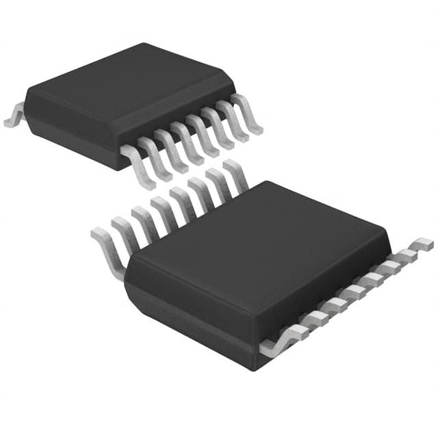
- Part No.:
- HV440WG-G
- Manufacturer:
- Microchip Technology
- Category:
- Telecom
- Package:
- 16-SOIC (0.295", 7.50mm Width)
- Datasheet:
-
 HV440WG-G.pdf
- Description:
- IC TELECOM INTERFACE 16SO
- Quantity:
- Payment:

- Shipping:

Inventory:4,722
Please send an inquiry. Send us your inquiry, and we will respond immediately.
Product details
Overview
HV440WG-G from Supertex Inc. is a high-voltage ring generator IC designed for telecom line interface applications, integrating P- and N-channel high-voltage transistors capable of delivering up to 70VRMS sine wave output at 15–60Hz into 5 North American REN loads, with pulse-by-pulse overcurrent protection set by external sense resistors and 100kHz PWM logic input compatibility.
For engineers reviewing the HV440WG-G datasheet, HV440WG-G pinout, HV440WG-G application, or HV440WG-G equivalent, key selection considerations include its 220V maximum operating voltage, dual high-voltage supply rails (VPP1 up to +110V, VNN1 down to –110V), 16-lead SOW (WG) package, and mode-selectable single- or dual-input control architecture.
Technical Context
The HV440WG-G implements independent logic-controlled gate drivers for internal high-voltage P- and N-channel transistors, with dedicated VPSEN and VNSEN inputs enabling per-cycle current limiting referenced to VPP1 and VNN1 respectively. Its internal linear regulators generate VPP2 (VPP1 −9.9V to VPP1 −19.1V) and VNN2 (VNN1 +5.6V to VNN1 +10.5V) for gate biasing.
Operation supports two control modes: when MODE = HIGH, PIN and NIN independently drive the P- and N-channel outputs; when MODE = LOW, NIN alone controls both channels with a fixed 200ns deadband to prevent shoot-through. EN is an active-low enable that forces HVOUT to high-impedance state.
Key Specifications
| Parameter | Value and Actual Design Meaning |
|---|---|
| VPP1 Range | +15V to +110V - sets positive high-voltage rail; determines maximum output swing amplitude |
| VNN1 Range | VPP1 −220V to −110V - defines negative high-voltage rail; enables bipolar ±110V output capability |
| Output Voltage | Up to 70VRMS sine wave - meets North American telephone ring signal standard for 5 REN load |
| Logic Supply | VDD = 4.5–5.5V - compatible with standard 5V microcontroller I/O without level shifting |
| Switching Frequency | Nominal 100kHz PWM input - supports precise timing control of ring waveform generation |
| Deadband Time | 200ns (MODE = LOW) - prevents cross-conduction during N- and P-channel transitions |
| Overcurrent Protection | Pulse-by-pulse via VPSEN/VNSEN - disables output within 100ns of fault detection |
Pinout & Package
Package: 16-lead SOW (Wide Body), 10.30 × 7.50 mm body, 2.65 mm max height, 1.27 mm pitch, RoHS-compliant (−G suffix).
| Pin/Terminal | Circuit Role | Design Meaning |
|---|---|---|
| 1 VPP1 | Positive high-voltage supply | Main positive rail input; must be decoupled and rated ≥110V |
| 2 PGND | High-voltage power ground | Return path for P-channel switching current; separate from low-voltage GND |
| 3 GND | Low-voltage logic ground | Reference for VDD, MODE, PIN, NIN, EN; must be isolated from PGND |
| 4 MODE | Control mode select | LOW enables single-input operation with 200ns deadband; HIGH enables dual-input control |
| 5 PIN | P-channel logic input | Active-HIGH disables internal P-channel; used only when MODE = HIGH |
| 6 NIN | N-channel logic input | Active-HIGH enables internal N-channel; functional in both MODE states |
| 7 EN | Active-low enable | Drives HVOUT to high-Z when asserted; overrides all other logic inputs |
| 8 VDD | Logic supply | 5V-tolerant digital supply; powers internal logic and level translators |
| 9 VNN1 | Negative high-voltage supply | Main negative rail input; must be decoupled and rated ≤−110V |
| 10 VNN2 | Negative gate regulator output | Internally generated gate bias for N-channel; requires 0.1µF bypass to VNN1 |
| 11 NGATE | External N-MOSFET driver | Drives TN2524N8 gate; extends output capability to 20 REN with external FETs |
| 12 VNSEN | N-channel current sense input | Monitors sink current via external resistor; triggers pulse-by-pulse shutdown if exceeded |
| 13 HVOUT | High-voltage output | Swings between VPP1 and VNN1; connects directly to telephone line transformer primary |
| 14 VPSEN | P-channel current sense input | Monitors source current via external resistor; enables symmetric overcurrent protection |
| 15 PGATE | External P-MOSFET driver | Drives TP2522N8 gate; required for 20 REN configuration with external FETs |
| 16 VPP2 | Positive gate regulator output | Internally generated gate bias for P-channel; requires 0.1µF bypass to VPP1 |
Key Features
| Feature | Design Value |
|---|---|
| Integrated high-voltage transistors | Eliminates need for discrete HV switches; reduces BOM count and layout complexity in ring generator designs |
| Dual independent current sense inputs | VPSEN and VNSEN allow asymmetric or matched sensing thresholds for P/N channel protection |
| Configurable control mode | Single-input (MODE = LOW) or dual-input (MODE = HIGH) operation simplifies MCU interface options |
| Internal linear regulators | VPP2 and VNN2 provide stable gate bias voltages without external LDOs, improving system efficiency |
| 220V absolute max rating | Supports robust operation under telecom surge conditions including lightning-induced transients |
Applications
| Telephone Line Interface | Set-Top Box Ring Generator |
|---|---|
Use Scenario: Generating standardized AC ring signal on POTS or VoIP gateway line cards. IC Role / Device Role / Timing Role: High-voltage analog waveform generator with precise RMS amplitude and frequency control. Use Value: Delivers compliant 70VRMS/20Hz ring signal into 5 REN load without external HV transistors or complex feedback loops. | Use Scenario: Providing ringing voltage to embedded telephony modules in cable or satellite STBs. IC Role / Device Role / Timing Role: Standalone ring signal source synchronized to host MCU commands. Use Value: Enables compact, low-cost ring generation using only two external sense resistors and no external HV FETs for basic 5 REN use. |
| Pair Gain System | Wireless Local Loop Base Station |
Use Scenario: Extending analog line reach in DSLAM or remote terminal pair gain equipment. IC Role / Device Role / Timing Role: High-reliability HV driver with pulse-by-pulse fault recovery for multi-line systems. Use Value: Survives repeated short-circuit events on shared lines due to fast 100ns overcurrent shutdown response. | Use Scenario: Ringing subscriber units in fixed wireless access base stations with limited board space. IC Role / Device Role / Timing Role: Integrated HV switch + gate drivers + regulators for minimal external component count. Use Value: Reduces bill-of-materials by integrating three critical functions (HV switching, gate drive, bias regulation) in one 16-pin SOW package. |
Equivalent & Alternatives
The following parts are listed as comparable options for similar high-voltage ring generator applications.
| Alternative Part | Technical Difference | Application Difference | Selection Advice |
|---|---|---|---|
| MAX14951A+T | Higher integration: includes integrated transformer driver and DC-DC converter; 3.3V logic compatible; no external sense resistors required | Targets newer VoIP/DECT systems requiring lower supply voltage and smaller footprint; lacks 20 REN external FET extension | Select MAX14951A+T for space-constrained 3.3V systems needing full integration; HV440WG-G remains preferred for legacy 5V designs requiring field-proven 20 REN scalability |
| UCC3911D | Lower voltage rating (±60V); no internal HV transistors - requires external HV FETs; no integrated gate regulators | Suitable for cost-sensitive designs where external FET selection is flexible; not drop-in for HV440WG-G's integrated HV switch topology | Choose UCC3911D when design flexibility and thermal management via discrete FETs are prioritized over integration and board area savings |
Compared with MAX14951A+T and UCC3911D, the HV440WG-G uniquely balances integration (internal HV transistors + gate regulators), legacy compatibility (5V logic, 5/20 REN support), and ruggedness (220V abs max, pulse-by-pulse protection), making it optimal for industrial telecom line cards requiring long-term availability and proven reliability.
Availability
HV440WG-G is available at Aetrix Electronics and suitable for telephone line interface, set-top box ring generation, and pair gain systems requiring stable component supply, long-lifecycle support, and RoHS-compliant packaging.
Supply support for HV440WG-G includes scheduled delivery planning, volume procurement assistance, BOM continuity management, traceable sourcing, and lifecycle availability coordination for OEM customers, industrial embedded developers, connected-device designers, and electronics production programs.
Manufacturer
Supertex Inc. was a U.S.-based semiconductor company specializing in high-voltage analog and mixed-signal ICs before its acquisition by Microchip Technology in 2014; known for robust, application-specific solutions in telecom and industrial markets.
The HV440WG-G belongs to Supertex's high-voltage ring generator product line, engineered specifically for reliable, low-component-count implementation of Bellcore GR-909-compliant telephone ringing signals in carrier-grade and CPE equipment.
FAQ
What is the maximum load capability of the HV440WG-G without external MOSFETs?
The HV440WG-G delivers up to 70VRMS sine wave output into a 5 North American REN load without external components. This is specified across the 15–60Hz frequency range with proper external filtering and transformer coupling. The device achieves this using its integrated high-voltage P- and N-channel transistors, eliminating the need for discrete HV switches in basic implementations. For higher loads up to 20 REN, the HV440WG-G requires two external MOSFETs: TN2524N8 (N-channel) and TP2522N8 (P-channel), driven via NGATE and PGATE pins.
How does the MODE pin affect control logic timing in the HV440WG-G?
When the MODE pin is pulled LOW, the HV440WG-G enters single-input mode where only the NIN signal controls both high-voltage transistors, with a fixed 200ns deadband enforced internally to prevent cross-conduction. When MODE is HIGH, PIN and NIN operate independently: PIN controls the P-channel (active-HIGH disables it), and NIN controls the N-channel (active-HIGH enables it). In either mode, the EN pin retains priority and forces HVOUT to high-impedance when asserted.
What are the absolute maximum voltage ratings for VPP1 and VNN1 on the HV440WG-G?
The HV440WG-G has an absolute maximum rating of +240V for the VPP1–VNN1 differential voltage, with individual limits of +120V on VPP1 and –170V on VNN1. However, for continuous operation, the recommended operating ranges are +15V to +110V for VPP1 and VPP1 −220V to –110V for VNN1. Exceeding these recommended ranges may compromise reliability or lifetime, even if below absolute maximums. These ratings reflect the device's suitability for telecom line interface applications subject to lightning and surge transients.
Can the HV440WG-G generate frequencies outside the 15–60Hz range?
The HV440WG-G is characterized and guaranteed to deliver compliant 70VRMS ring signals within the 15–60Hz range into 5 REN loads, aligning with North American telephone standards. While the internal PWM logic accepts 100kHz inputs and the output stage can switch faster, performance outside this band-especially at lower frequencies (<15Hz) or higher frequencies (>60Hz)-is not specified for amplitude accuracy, distortion, or thermal stability. Applications requiring non-standard frequencies should validate output waveform fidelity, THD, and thermal behavior under actual load conditions.
What external components are mandatory for basic HV440WG-G operation?
Four external components are mandatory for basic HV440WG-G operation: (1) a 0.1µF capacitor between VPP2 and VPP1, (2) a 0.1µF capacitor between VNN2 and VNN1, (3) two current sense resistors connected to VPSEN and VNSEN for overcurrent protection, and (4) output filtering (e.g., 1.5mH inductor + 4.3Ω/0.22µF network) to shape the sine wave. Additional components like gate resistors or transformer coupling depend on system-level requirements but are not strictly mandatory for functional evaluation.
HV440WG-G Specifications
- Product attributes
- Attribute value
- Manufacturer:
- Microchip Technology
- Series:
- -
- Package/Case:
- 16-SOIC (0.295", 7.50mm Width)
- Packaging:
- Tape & Reel (TR)
- Product Status:
- Obsolete
- Function:
- Ring Generator Controller
- Interface:
- -
- Number of Circuits:
- 1
- Voltage - Supply:
- 15V ~ 110V
- Current - Supply:
- 1.9mA
- Power (Watts):
- -
- Operating Temperature:
- -
- Grade:
- -
- Qualification:
- -
- Mounting Type:
- Surface Mount
- Supplier Device Package:
- 16-SO
HV440WG-G FAQ
1.How can I place an order for HV440WG-G through Aetrix?
Please submit a Request for Quotation (RFQ) for HV440WG-G on Aetrix. Our sales agent will provide a competitive quotation and guide you through the order confirmation once you accept the terms.
2.Are the price and stock information for HV440WG-G reliable?
The price and inventory of HV440WG-G are updated periodically and may fluctuate due to market conditions. Stock and pricing data are typically refreshed every 24 hours. Quotation validity for HV440WG-G is usually 5 days.
3.What payment methods are accepted for HV440WG-G?
We accept Wire Transfer, PayPal, Credit Card, Western Union, MoneyGram, and Escrow for HV440WG-G transactions.
Note: Certain payment methods may incur a processing fee.
4.How is shipping managed for HV440WG-G?
HV440WG-G orders can be shipped via leading logistics carriers, including DHL, UPS, FedEx, TNT, or Registered Mail.
Once your HV440WG-G order is processed, you will receive an email with the shipment details and tracking number.
Note: Tracking information may take up to 24 hours to appear. Express delivery typically takes 3–5 business days.
5.How can I obtain technical support or documentation for HV440WG-G?
For technical support, including HV440WG-G datasheets, pinout diagrams, or application guidance, please contact our engineering support team. They can provide detailed documentation and assistance for your HV440WG-G requirements.
6.How does Aetrix verify that HV440WG-G is sourced from the original manufacturer or authorized distributors?
All HV440WG-G products on Aetrix are procured from qualified distributors and authorized channels. Our dedicated quality assurance team conducts strict verification, including traceability checks and, if necessary, third-party testing. This ensures that HV440WG-G meets industry standards.
7.What is the process for return or replacement of HV440WG-G?
All HV440WG-G units undergo pre-shipment inspection (PSI). If there is an issue with HV440WG-G, returns or replacements are accepted under the following conditions:
1.Quantity discrepancies, incorrect items, or visible external defects (such as breakage or corrosion), acknowledged by Aetrix.
2.The issue is reported within 90 days of delivery.
3.The HV440WG-G part is unused and in its original packaging.
Return procedure for HV440WG-G:
1.Submit a request within 90 days.
2.Obtain a Return Material Authorization (RMA) from Aetrix.
HV440WG-G Tags

-
LMC567CMX/NOPB
Texas Instruments
-
LM567CMX/NOPB
Texas Instruments
-
LM567CM/NOPB
Texas Instruments

-
VSC8531XMW-02
Microchip Technology
-
VSC8531XMW-05
Microchip Technology

-
GPY115C0VI
MaxLinear, Inc.

-
SI32185-A-FMR
Skyworks Solutions Inc.

-
VSC8541XMV-05
Microchip Technology

-
SI32178-B-FM1R
Skyworks Solutions Inc.
-
GPY215C0VI
MaxLinear, Inc.

-
CPC7514ZTR
Littelfuse Inc.

-
VSC8502XML-03
Microchip Technology
Tech Hub

TTL and CMOS logic families differ in thresholds, loading, output drive, power and timing. This engineering guide compares 74HC and 74HCT, calculates noise margins and checks 3.3 V/5 V compatibility.

A practical engineering guide to 3.3V and 5V logic compatibility, input thresholds, resistor dividers, translator ICs, MOSFET level shifting, I2C pull-ups, timing limits and power-sequencing risks.

The 74HC595 uses push-pull logic outputs, while the TPIC6B595 uses 50 V open-drain DMOS sinks for higher-power loads. This guide compares timing, current limits, 3.3 V interfacing, load wiring, thermal…

The 74HC595 converts serial data into eight stable parallel outputs. This guide covers pin functions, shift and storage timing, OE and MR behavior, drive-current limits, cascading, voltage compatibilit…

A technical comparison of level-sensitive latches and edge-triggered flip-flops, covering timing windows, setup and hold limits, master–slave operation, time borrowing, race-through, HDL inference and…

A D latch stores one bit while Enable controls when data can pass. This reference covers gate-level operation, truth tables, transparency, setup and hold timing, LE versus OE, common ICs and practical …

An SR latch stores one bit through cross-coupled feedback. This engineering reference covers NOR and NAND implementations, truth tables, forbidden-state recovery, gated operation, switch debouncing, fa…

Latch circuits retain one bit through feedback. This technical reference covers SR and D latches, truth tables, transparency, timing limits, latch-versus-flip-flop behavior, applications and common log…

An engineering guide to LED driver operation, constant-current and constant-voltage outputs, linear and switching topologies, dimming, IC selection, calculations, replacement compatibility, and fault c…

Operational amplifier guide covering op amp basics, feedback, ideal vs real op amps, common configurations, buffer circuits, offset, bias current, gain-bandwidth, slew rate, rail-to-rail limits and sel…


