
 My Inquiry
 My Account


Microchip Technology HV461FG-G
- Part No.:
- HV461FG-G
- Manufacturer:
- Microchip Technology
- Category:
- Telecom
- Package:
- 48-LQFP
- Datasheet:
-
 HV461FG-G.pdf
- Description:
- IC TELECOM INTERFACE 48LQFP
- Quantity:
- Payment:

- Shipping:

Inventory:2,841
Please send an inquiry. Send us your inquiry, and we will respond immediately.
Product details
Overview
HV461FG-G from Supertex Inc. is a ring generator controller IC designed for telecom -48V-powered ringer circuits, delivering digitally programmable 94VAC (rms) sine-wave output with 12–63Hz frequency range, ±0.1% frequency accuracy, and 80% typical system efficiency driving up to 40 REN loads.
For engineers reviewing the HV461FG-G datasheet, HV461FG-G pinout, HV461FG-G application, or HV461FG-G equivalent, this page provides verified technical context, validated pin functions, confirmed telecom-specific timing roles, and real-world design meaning for PBX, DLC, and wireless loop systems.
Technical Context
The HV461FG-G integrates an 8-frequency sine wave synthesizer (12–63Hz), digital amplitude/offset control via AMP0–1 and OFF0–1 inputs, and a synchronous 4-quadrant inverter controller with zero-cross turn-on capability. It supports both open-loop and closed-loop operation using internal error amplifiers and external current-sense feedback.
Its architecture includes an internal boost converter (9.6V typical VGD output), programmable PWM frequency (21.25–172.5kHz), adjustable primary deadband (tDB) and secondary delay (tDLY), and fault detection covering overcurrent, VDD/VGD undervoltage, and PWM overrange - all coordinated through a transparent latch and ENABLE/SYNC logic.
Key Specifications
| Parameter | Value and Actual Design Meaning |
|---|---|
| VDD Supply | 3.0–3.6V; powers analog/digital sections with 7–30mA total current draw at 100kHz PWM. |
| Ringer Output | 94VAC (rms), floating, programmable DC offset (0–±94V) and amplitude (0–100% full scale). |
| Frequency Range | 12–63Hz; eight factory-set frequencies (e.g., 16.7, 20, 25, 33.3, 40, 50, 60Hz) plus external FRING input. |
| THD | <3% at 16.7–60Hz with 33nF CSINE; ensures clean sine waveform for telecom compliance. |
| Reference Voltages | VREF1 = 1.25V ±3.5mV (200µV/°C TC); VREF2 = 2.50V ±12.5mV; used for gain/offset calibration and current limit. |
| SYNC Lead Time | Adjustable 4.5–5.5ms via TSYNC RC network; enables precise synchronization of ringing relays. |
| FAULT Detection | Activates on >8% PWM overrange/overcurrent or immediate VDD/VGD undervoltage; open-drain active-low output. |
Pinout & Package
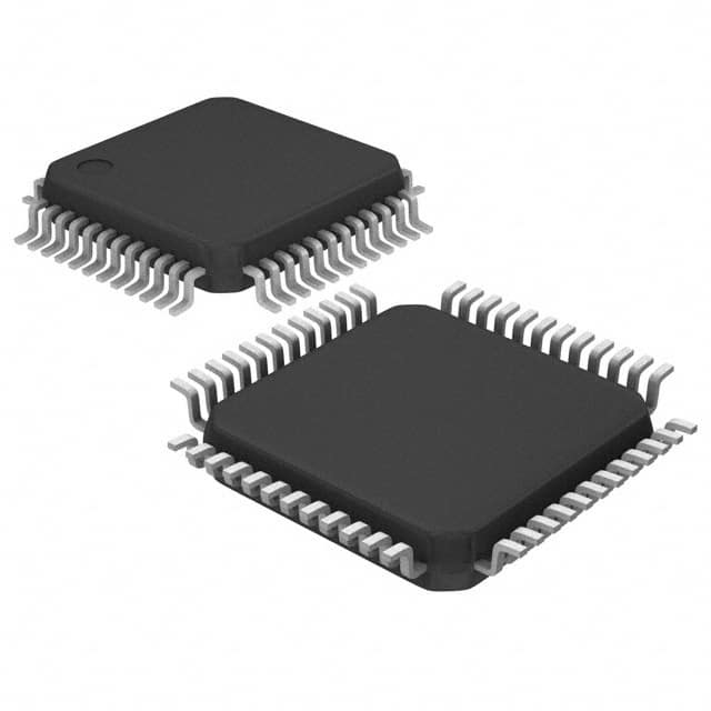
HV461FG-G is housed in a 48-lead LQFP package (7.0×7.0mm body, 0.5mm pitch, 1.6mm max height), RoHS-compliant and marked "HV461FG" with year/week/lot codes.
| Pin/Terminal | Circuit Role | Design Meaning |
|---|---|---|
| 1, 47–48 | DCREFx | DC offset reference inputs; selected by OFF0/OFF1 to set ringer output DC bias level. |
| 2–3 | VREF1 / VREF2 | Precision 1.25V/2.50V references; bypassed with 100nF caps for stable gain/offset calibration. |
| 9 | ROSC | Sets PWM frequency (21.25–172.5kHz) via resistor to VDD; determines inverter switching speed. |
| 14 | SYNC | Digital 0°/180° phase crossing indicator; lead time adjustable via TSYNC RC for relay sync timing. |
| 16 | ENABLE | Active-high ringer enable; forces 0° start on activation and disables output during reset or fault. |
| 21–23 | FREQ0–FREQ2 | 3-bit bus selecting one of eight built-in ring frequencies; changes take effect at next phase crossing. |
| 28–31 | SW1–SW4 | Gate drivers for 4-quadrant inverter: SW1/SW2 (primary P/N-MOSFETs), SW3/SW4 (secondary rectifiers). |
| 33–34 | VGD / VDR | VGD supplies 9.6V gate drive; VDR drives external boost converter with fixed 50% duty cycle at PWM frequency. |
Key Features
| Feature | Design Value |
|---|---|
| Digital ring control | Independent 3-bit frequency (FREQ0–2), 2-bit amplitude (AMP0–1), and 2-bit offset (OFF0–1) selection with phase-aligned updates. |
| Efficient 4-quadrant topology | Enables >80% system efficiency by synchronizing primary inverter and secondary rectifier switching with programmable deadband (tDB) and delay (tDLY). |
| Programmable SYNC timing | Configurable 4.5–5.5ms lead time via TSYNC RC network ensures reliable mechanical relay actuation without contact bounce. |
| Robust fault protection | Integrated detection of overcurrent, VDD/VGD undervoltage, and PWM overrange - each triggering open-drain FAULT output within microseconds. |
| Flexible power stage interface | Separate AVDD/DVDD supplies with shared ground; VGD-regulated gate drive; CL+/CL− current sense inputs with COMP1/COMP2 compensation pins. |
Applications
| Telecom PBX Systems | DLC Remote Terminals |
|---|---|
Use Scenario: Central office PBX generating ring signals for analog telephone lines. IC Role / Device Role / Timing Role: Ring generator controller managing sine synthesis, amplitude/offset programming, and synchronized relay actuation via SYNC output. Use Value: Delivers compliant 94VAC (rms), low-THD ringing at selectable frequencies (e.g., 20Hz or 25Hz) with precise 0°-phase start and adjustable lead time for relay timing. |
Use Scenario: Digital Loop Carrier remote terminal powering multiple subscriber lines over copper pairs. IC Role / Device Role / Timing Role: High-efficiency ringer controller driving up to 40 REN load with programmable DC offset to match line voltage referencing requirements. Use Value: Achieves >80% efficiency using synchronous rectification and 4-quadrant topology, reducing thermal load in space-constrained DLC cabinets. |
| Wireless Loop Base Stations | Enterprise Key Systems |
Use Scenario: Wireless local loop base station providing PSTN-compatible ringing to cordless handsets. IC Role / Device Role / Timing Role: Programmable ring controller accepting external FRING input for custom frequencies and supporting AC-only, AC+DC, or DC-only output modes. Use Value: Enables frequency agility (12–63Hz) and flexible output configuration (e.g., AC+DC offset) to meet regional telecom standards without hardware change. |
Use Scenario: Business telephone key system requiring multi-line ringing with independent amplitude/offset control per port. IC Role / Device Role / Timing Role: Digital ring controller interfacing with host MCU via 8-bit bus or individual logic inputs for per-line ringer parameter configuration. Use Value: Transparent latch (LE pin) allows simultaneous update of FREQ/AMP/OFF across multiple HV461FG-G units for synchronized multi-line ringing. |
Equivalent & Alternatives
The following parts are listed as comparable options for similar ring generator controller applications.
| Alternative Part | Technical Difference | Application Difference | Selection Advice |
|---|---|---|---|
| MAX13242E | Single-chip solution with integrated MOSFET drivers and 100V H-bridge; no external boost required; lower integration of reference/PLL circuitry. | Targeted at lower-RMS-voltage (≤60VAC), lower-REN (<15) applications; lacks programmable SYNC lead time and 4-quadrant topology. | Preferred for compact, low-power designs where 94VAC/40REN capability is not required. |
| TI UCC38C43 | Current-mode PWM controller with external oscillator; requires discrete sine synthesis, amplitude/offset DACs, and separate fault logic. | Demands full custom implementation of ring waveform generation, current sensing, and protection - significantly higher BOM and layout complexity. | Selected only when full architectural flexibility is needed and design resources support full analog/digital co-design. |
Compared with MAX13242E and UCC38C43, the HV461FG-G uniquely combines programmable 94VAC sine synthesis, 4-quadrant synchronous rectification control, and telecom-grade SYNC timing in a single 48-pin LQFP - eliminating external DACs, op-amps, and discrete protection circuitry while enabling 40 REN drive capability.
Availability
HV461FG-G is available at Aetrix Electronics and suitable for telecom PBX systems, digital loop carrier (DLC) terminals, and wireless loop infrastructure requiring stable component supply, long-lifecycle support, and RoHS-compliant packaging.
Supply support for HV461FG-G includes scheduled delivery planning, volume procurement assistance, BOM continuity management, traceable sourcing, and lifecycle availability coordination for OEM customers, industrial embedded developers, connected-device designers, and electronics production programs.
Manufacturer
Supertex Inc. was a fabless semiconductor company specializing in high-voltage analog and power management ICs, acquired by Microchip Technology in 2014.
The HV461FG-G belongs to Supertex's telecom ring generator controller product line, engineered specifically for efficient, programmable -48V-powered ringer circuits in PBX, DLC, and key system applications.
FAQ
What is the maximum load drive capability of the HV461FG-G?
The HV461FG-G supports up to 40 Ringer Equivalence Number (REN) load when used with the patented 4-quadrant inverter topology and synchronous rectifiers. This corresponds to approximately 94VAC (rms) into a 1.2kΩ resistive load at 20Hz, achieving >80% typical system efficiency. Load capability assumes proper external power stage design per Figure 6 in the DSFP-HV461 datasheet.
How does the HV461FG-G achieve zero-cross turn-on?
The HV461FG-G achieves zero-cross turn-on through its internal sine wave synthesizer and transparent latch architecture: when ENABLE transitions high, the ringer output starts precisely at 0° phase of the synthesized sine wave. This behavior is guaranteed regardless of FREQ/AMP/OFF setting and is independent of external crystal jitter due to digital phase alignment logic inside the HV461FG-G.
Can the HV461FG-G generate non-standard ring frequencies outside the eight built-in options?
Yes, the HV461FG-G accepts an external logic-level signal on the FRING pin (Pin 7) to set arbitrary ring frequencies from 12Hz to 63Hz at a 1:1 ratio. The internal synthesizer locks to this input while preserving amplitude and offset control via AMP0–1 and OFF0–1. Phase synchronization to the external signal is not maintained - enabling immediate 0° start upon ENABLE assertion.
What is the function of the TSYNC pin on the HV461FG-G?
The TSYNC pin (Pin 5) sets the SYNC pulse lead time - the interval between the rising edge of the SYNC output (Pin 14) and the actual 0°/180° phase crossing of the sine reference. Using an RC network (tLEAD ≈ 0.48·R·C), designers configure 4.5–5.5ms lead time to ensure mechanical ringing relays close before voltage peaks, preventing contact arcing and extending relay life in HV461FG-G-based systems.
Does the HV461FG-G require external components for fault protection?
No, the HV461FG-G integrates comprehensive fault protection: overcurrent detection via CL+/CL− inputs, VDD and VGD undervoltage lockout, and PWM overrange monitoring. The FAULT pin (Pin 15) asserts active-low under any of these conditions. Only an external CFAULT capacitor (1–100µF) is required to set integration time - no additional comparators, timers, or logic gates are needed for basic protection in HV461FG-G designs.
HV461FG-G Specifications
- Product attributes
- Attribute value
- Manufacturer:
- Microchip Technology
- Series:
- -
- Package/Case:
- 48-LQFP
- Packaging:
- Tray
- Product Status:
- Obsolete
- Function:
- Ring Generator Controller
- Interface:
- -
- Number of Circuits:
- 1
- Voltage - Supply:
- 3V ~ 3.6V
- Current - Supply:
- 7mA
- Power (Watts):
- -
- Operating Temperature:
- -40°C ~ 85°C
- Grade:
- -
- Qualification:
- -
- Mounting Type:
- Surface Mount
- Supplier Device Package:
- 48-LQFP (7x7)
HV461FG-G FAQ
1.How can I place an order for HV461FG-G through Aetrix?
Please submit a Request for Quotation (RFQ) for HV461FG-G on Aetrix. Our sales agent will provide a competitive quotation and guide you through the order confirmation once you accept the terms.
2.Are the price and stock information for HV461FG-G reliable?
The price and inventory of HV461FG-G are updated periodically and may fluctuate due to market conditions. Stock and pricing data are typically refreshed every 24 hours. Quotation validity for HV461FG-G is usually 5 days.
3.What payment methods are accepted for HV461FG-G?
We accept Wire Transfer, PayPal, Credit Card, Western Union, MoneyGram, and Escrow for HV461FG-G transactions.
Note: Certain payment methods may incur a processing fee.
4.How is shipping managed for HV461FG-G?
HV461FG-G orders can be shipped via leading logistics carriers, including DHL, UPS, FedEx, TNT, or Registered Mail.
Once your HV461FG-G order is processed, you will receive an email with the shipment details and tracking number.
Note: Tracking information may take up to 24 hours to appear. Express delivery typically takes 3–5 business days.
5.How can I obtain technical support or documentation for HV461FG-G?
For technical support, including HV461FG-G datasheets, pinout diagrams, or application guidance, please contact our engineering support team. They can provide detailed documentation and assistance for your HV461FG-G requirements.
6.How does Aetrix verify that HV461FG-G is sourced from the original manufacturer or authorized distributors?
All HV461FG-G products on Aetrix are procured from qualified distributors and authorized channels. Our dedicated quality assurance team conducts strict verification, including traceability checks and, if necessary, third-party testing. This ensures that HV461FG-G meets industry standards.
7.What is the process for return or replacement of HV461FG-G?
All HV461FG-G units undergo pre-shipment inspection (PSI). If there is an issue with HV461FG-G, returns or replacements are accepted under the following conditions:
1.Quantity discrepancies, incorrect items, or visible external defects (such as breakage or corrosion), acknowledged by Aetrix.
2.The issue is reported within 90 days of delivery.
3.The HV461FG-G part is unused and in its original packaging.
Return procedure for HV461FG-G:
1.Submit a request within 90 days.
2.Obtain a Return Material Authorization (RMA) from Aetrix.
HV461FG-G Tags

-
LMC567CMX/NOPB
Texas Instruments
-
LM567CMX/NOPB
Texas Instruments
-
LM567CM/NOPB
Texas Instruments

-
VSC8531XMW-02
Microchip Technology
-
VSC8531XMW-05
Microchip Technology

-
GPY115C0VI
MaxLinear, Inc.

-
SI32185-A-FMR
Skyworks Solutions Inc.

-
VSC8541XMV-05
Microchip Technology

-
SI32178-B-FM1R
Skyworks Solutions Inc.
-
GPY215C0VI
MaxLinear, Inc.

-
CPC7514ZTR
Littelfuse Inc.

-
VSC8502XML-03
Microchip Technology
Tech Hub

TTL and CMOS logic families differ in thresholds, loading, output drive, power and timing. This engineering guide compares 74HC and 74HCT, calculates noise margins and checks 3.3 V/5 V compatibility.

A practical engineering guide to 3.3V and 5V logic compatibility, input thresholds, resistor dividers, translator ICs, MOSFET level shifting, I2C pull-ups, timing limits and power-sequencing risks.

The 74HC595 uses push-pull logic outputs, while the TPIC6B595 uses 50 V open-drain DMOS sinks for higher-power loads. This guide compares timing, current limits, 3.3 V interfacing, load wiring, thermal…

The 74HC595 converts serial data into eight stable parallel outputs. This guide covers pin functions, shift and storage timing, OE and MR behavior, drive-current limits, cascading, voltage compatibilit…

A technical comparison of level-sensitive latches and edge-triggered flip-flops, covering timing windows, setup and hold limits, master–slave operation, time borrowing, race-through, HDL inference and…

A D latch stores one bit while Enable controls when data can pass. This reference covers gate-level operation, truth tables, transparency, setup and hold timing, LE versus OE, common ICs and practical …

An SR latch stores one bit through cross-coupled feedback. This engineering reference covers NOR and NAND implementations, truth tables, forbidden-state recovery, gated operation, switch debouncing, fa…

Latch circuits retain one bit through feedback. This technical reference covers SR and D latches, truth tables, transparency, timing limits, latch-versus-flip-flop behavior, applications and common log…

An engineering guide to LED driver operation, constant-current and constant-voltage outputs, linear and switching topologies, dimming, IC selection, calculations, replacement compatibility, and fault c…

Operational amplifier guide covering op amp basics, feedback, ideal vs real op amps, common configurations, buffer circuits, offset, bias current, gain-bandwidth, slew rate, rail-to-rail limits and sel…


