
 My Inquiry
 My Account


Skyworks Solutions Inc. HY92-12LF
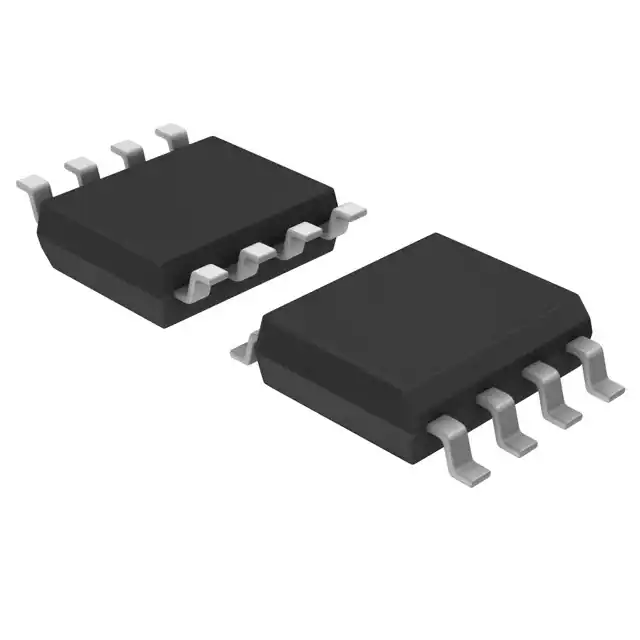
- Part No.:
- HY92-12LF
- Manufacturer:
- Skyworks Solutions Inc.
- Category:
- RF Directional Coupler
- Package:
- 8-SOIC (0.154", 3.90mm Width)
- Datasheet:
-
 HY92-12LF.pdf
- Description:
- RF DIR COUPLER 880-960MHZ 8SOIC
- Quantity:
- Payment:

- Shipping:

Inventory:4,594
Please send an inquiry. Send us your inquiry, and we will respond immediately.
Product details
Overview
HY92-12LF from Skyworks Solutions is a monolithic 90-degree hybrid coupler designed for RF power splitting and combining in the 0.88–0.96 GHz band, featuring 0.5 dB typical insertion loss, 25 dB typical isolation, ±0.8 dB amplitude balance, ±2° phase balance, and SOIC-8 surface-mount packaging. It serves as a passive divider/coupler in cellular infrastructure transceivers requiring precise quadrature signal distribution.
For engineers reviewing the HY92-12LF datasheet, HY92-12LF pinout, HY92-12LF application, or HY92-12LF equivalent, key selection criteria include its guaranteed 0.88–0.96 GHz bandwidth, 4 W input power handling, RoHS-compliant lead-free construction, and symmetric 4-port configuration enabling flexible port assignment in RF front-end designs.
Technical Context
This device implements a passive, monolithic 90° hybrid architecture with no active components, delivering fixed-phase quadrature outputs between coupled and direct ports. Its performance is specified at 50 Ω impedance and 25 °C ambient, with all ports exhibiting matched VSWR ≤1.2:1 across the band.
The HY92-12LF supports bidirectional operation due to inherent symmetry: any non-ground pin (1, 4, 5, or 8) may serve as input, with corresponding termination and output assignments defined per the datasheet's port mapping table. Ground pins (2, 3, 6, 7) are internally connected and must be soldered to PCB ground planes.
Key Specifications
| Parameter | Value and Actual Design Meaning |
|---|---|
| Frequency Range | 0.88–0.96 GHz: Full specification compliance across entire cellular UMTS Band IX / LTE Band 8 transmit window. |
| Insertion Loss | 0.5 dB typ.: Represents net path loss from input to direct port, excluding 3 dB theoretical split loss. |
| Isolation | 25 dB typ.: Minimum signal rejection between input and isolated port, critical for transmitter leakage suppression. |
| Amplitude Balance | ±0.8 dB max.: Tolerance between direct and coupled output power levels, enabling accurate I/Q signal generation. |
| Phase Balance | ±2° max.: Deviation from ideal 90° quadrature between coupled and direct outputs, limiting image rejection in modulators. |
| Input Power | 4 W max.: Continuous RF power handling capability without degradation, supporting high-efficiency PA output stages. |
| VSWR (All Ports) | 1.2:1 max.: Ensures <10% reflected power at each port under matched 50 Ω conditions. |
Pinout & Package
HY92-12LF uses an SOIC-8 surface-mount package (5.00 × 4.00 mm footprint, 1.24 mm body height) with gull-wing leads and MSL-1 moisture sensitivity rating. All ground pins are internally tied and require external PCB grounding.
| Pin/Terminal | Circuit Role | Design Meaning |
|---|---|---|
| 1 | RF Input | Primary RF signal entry point; may be reassigned as direct or coupled output per symmetric configuration. |
| 2 | GND | Internally connected ground terminal; must be soldered to PCB ground plane for thermal and RF stability. |
| 3 | ISOL. | Isolated port requiring 50 Ω termination to absorb reflected energy and maintain isolation spec. |
| 4 | GND | Internally connected ground terminal; identical function and connectivity to Pin 2. |
| 5 | Direct | Main output port with 0° phase relative to input; used for carrier or LO paths in quadrature architectures. |
| 6 | GND | Internally connected ground terminal; identical function and connectivity to Pins 2 and 4. |
| 7 | GND | Internally connected ground terminal; fourth ground connection for low-inductance RF return path. |
| 8 | Coupled | Quadrature output port with 90° phase shift; paired with Pin 5 for I/Q signal generation or antenna diversity switching. |
Key Features
| Feature | Design Value |
|---|---|
| Monolithic passive construction | Eliminates discrete component variation and assembly tolerances, ensuring repeatable amplitude/phase balance across production lots. |
| SOIC-8 surface-mount package | Enables automated placement and reflow in high-volume RF module assembly, with 1.24 mm profile suitable for space-constrained baseband boards. |
| Lead-free and RoHS-compliant | Meets JEDEC J-STD-020 MSL-1 requirements for 260 °C peak reflow, eliminating Pb-based solder compatibility concerns. |
| Symmetric 4-port topology | Allows field-reconfigurable use as splitter, combiner, or 90° hybrid without hardware change-input can be assigned to Pins 1, 4, 5, or 8. |
Applications
| Cellular Base Station Transceivers | UMTS/LTE Power Amplifier Feedback |
|---|---|
Use Scenario: Quadrature signal generation for I/Q upconversion in macrocell BTS transmit chains operating at 900 MHz. IC Role / Device Role / Timing Role: 90° hybrid coupler providing phase-orthogonal RF paths to dual-channel DAC-driven mixers. Use Value: ±2° phase balance ensures >35 dB image rejection, meeting 3GPP ACLR requirements for adjacent channel leakage. | Use Scenario: Coupling a portion of PA output for envelope tracking or digital predistortion (DPD) feedback loops. IC Role / Device Role / Timing Role: Passive directional coupler extracting 3 dB sampled signal with minimal insertion loss to preserve PA efficiency. Use Value: 0.5 dB typical insertion loss minimizes forward-path degradation while 25 dB isolation prevents feedback instability. |
| ISM Band Wireless Access Points | RF Test & Calibration Systems |
Use Scenario: Antenna diversity switching in 902–928 MHz ISM-band Wi-Fi access points using dual-RF-chain receivers. IC Role / Device Role / Timing Role: Signal splitter routing common IF/RF source to two parallel receiver paths with matched group delay. Use Value: ±0.8 dB amplitude balance maintains consistent SNR across diversity branches, improving fade margin by ≥3 dB. | Use Scenario: Reference signal distribution in automated RF test fixtures verifying transceiver EVM and spectral mask compliance. IC Role / Device Role / Timing Role: Precision power splitter delivering phase-coherent stimulus signals to multiple DUT inputs simultaneously. Use Value: 1.2:1 VSWR across all ports ensures minimal mismatch uncertainty (<0.1 dB) in calibrated measurement setups. |
Equivalent & Alternatives
The following parts are listed as comparable options for similar 90-degree hybrid coupler applications.
| Alternative Part | Technical Difference | Application Difference | Selection Advice |
|---|---|---|---|
| Qorvo QPB9050 | 0.7–1.0 GHz range; 0.6 dB insertion loss; SOIC-8; requires external 50 Ω termination on isolated port. | Broader bandwidth but looser phase balance (±3.5°), less suitable for high-accuracy I/Q modulation. | Select when wider frequency coverage is prioritized over quadrature fidelity in non-critical feedback paths. |
| Analog Devices ADL5572 | 0.8–1.0 GHz; integrated active amplifier; 16-QFN package; +5 V supply required. | Active gain (+13 dB) replaces passive loss, but introduces noise figure penalty and DC power dependency. | Select only when system-level gain budget is insufficient to tolerate 3.5 dB passive split loss. |
Compared with QPB9050 and ADL5572, the HY92-12LF delivers superior phase accuracy and zero power consumption in a drop-in SOIC-8 footprint, making it optimal for passive RF signal routing where quadrature integrity and thermal stability are primary design constraints.
Availability
HY92-12LF is available at Aetrix Electronics and suitable for cellular infrastructure, wireless access point development, and RF test equipment requiring stable component supply with full traceability and long-term lifecycle support.
Supply support for HY92-12LF includes scheduled delivery planning, volume procurement assistance, BOM continuity management, traceable sourcing, and lifecycle availability coordination for OEM customers, industrial embedded developers, connected-device designers, and electronics production programs.
Manufacturer
Skyworks Solutions is a global leader in high-performance analog semiconductors, specializing in RF, mobile, and infrastructure solutions with emphasis on integration and power efficiency.
The HY92-12LF belongs to Skyworks' monolithic hybrid coupler product line, engineered specifically for precision RF signal division and combining in sub-1 GHz wireless infrastructure applications.
FAQ
What is the maximum RF input power rating for HY92-12LF?
The HY92-12LF has an absolute maximum input power rating of 4 W continuous RF power, verified under 25 °C ambient and 50 Ω matched conditions. Exceeding this limit risks irreversible damage to the monolithic passive structure. Derating is recommended above 25 °C per the device's thermal resistance profile, and actual system-level power handling must account for VSWR-induced standing waves at the input port.
Can HY92-12LF be used as both a splitter and a combiner?
Yes, the HY92-12LF operates bidirectionally due to its symmetric monolithic architecture. When used as a combiner, applying equal-amplitude, 90°-phase-shifted signals to the Direct (Pin 5) and Coupled (Pin 8) ports produces a summed output at Pin 1, while Pin 3 must remain terminated. Performance metrics-including isolation and amplitude balance-remain valid in reverse operation per the datasheet's port mapping table.
Does HY92-12LF require external bias or control signals?
No, the HY92-12LF is a fully passive monolithic device with no DC power connections, control pins, or bias circuitry. It functions solely through distributed RF coupling and requires only proper 50 Ω terminations on all ports except the intended input and outputs. This eliminates power supply design complexity and enables operation across extreme temperature ranges (–40 °C to +85 °C).
What is the significance of the "LF" suffix in HY92-12LF?
The "LF" suffix in HY92-12LF denotes lead-free and RoHS-compliant construction per JEDEC J-STD-020 MSL-1 standards, with peak reflow tolerance up to 260 °C. It distinguishes this variant from legacy leaded versions and confirms compliance with environmental regulations for commercial and industrial electronics manufacturing.
How does the SOIC-8 package of HY92-12LF impact PCB layout?
The HY92-12LF's SOIC-8 footprint (5.00 × 4.00 mm) requires strict adherence to Skyworks' recommended board layout: solid ground plane beneath the device, 12 thermal vias under the exposed pad area (Pins 2/3/4/6/7), and controlled-impedance 50 Ω traces with minimized stub length. Deviations increase VSWR and degrade amplitude/phase balance beyond datasheet limits.
HY92-12LF Specifications
- Product attributes
- Attribute value
- Manufacturer:
- Skyworks Solutions Inc.
- Series:
- -
- Packaging:
- Tape & Reel (TR)
- Product Status:
- Obsolete
- Coupler Type:
- Standard
- Frequency:
- 880MHz ~ 960MHz
- Coupling Factor:
- -
- Applications:
- General Purpose
- Insertion Loss:
- 0.4dB
- Power - Max:
- 4W
- Isolation:
- 25dB
- Return Loss:
- 26dB
- Supplier Device Package:
- 8-SOIC
HY92-12LF FAQ
1.How can I place an order for HY92-12LF through Aetrix?
Please submit a Request for Quotation (RFQ) for HY92-12LF on Aetrix. Our sales agent will provide a competitive quotation and guide you through the order confirmation once you accept the terms.
2.Are the price and stock information for HY92-12LF reliable?
The price and inventory of HY92-12LF are updated periodically and may fluctuate due to market conditions. Stock and pricing data are typically refreshed every 24 hours. Quotation validity for HY92-12LF is usually 5 days.
3.What payment methods are accepted for HY92-12LF?
We accept Wire Transfer, PayPal, Credit Card, Western Union, MoneyGram, and Escrow for HY92-12LF transactions.
Note: Certain payment methods may incur a processing fee.
4.How is shipping managed for HY92-12LF?
HY92-12LF orders can be shipped via leading logistics carriers, including DHL, UPS, FedEx, TNT, or Registered Mail.
Once your HY92-12LF order is processed, you will receive an email with the shipment details and tracking number.
Note: Tracking information may take up to 24 hours to appear. Express delivery typically takes 3–5 business days.
5.How can I obtain technical support or documentation for HY92-12LF?
For technical support, including HY92-12LF datasheets, pinout diagrams, or application guidance, please contact our engineering support team. They can provide detailed documentation and assistance for your HY92-12LF requirements.
6.How does Aetrix verify that HY92-12LF is sourced from the original manufacturer or authorized distributors?
All HY92-12LF products on Aetrix are procured from qualified distributors and authorized channels. Our dedicated quality assurance team conducts strict verification, including traceability checks and, if necessary, third-party testing. This ensures that HY92-12LF meets industry standards.
7.What is the process for return or replacement of HY92-12LF?
All HY92-12LF units undergo pre-shipment inspection (PSI). If there is an issue with HY92-12LF, returns or replacements are accepted under the following conditions:
1.Quantity discrepancies, incorrect items, or visible external defects (such as breakage or corrosion), acknowledged by Aetrix.
2.The issue is reported within 90 days of delivery.
3.The HY92-12LF part is unused and in its original packaging.
Return procedure for HY92-12LF:
1.Submit a request within 90 days.
2.Obtain a Return Material Authorization (RMA) from Aetrix.
HY92-12LF Tags
.jpg)
-
C0810J5003AHF
TTM Technologies, Inc.
-
C5060J5003AHF
TTM Technologies, Inc.
-
C1517J5003AHF
TTM Technologies, Inc.
-
DC0710J5010AHF
TTM Technologies, Inc.
-
DC2337J5020AHF
TTM Technologies, Inc.
-
C0727J5003AHF
TTM Technologies, Inc.
-
DC2337J5010AHF
TTM Technologies, Inc.

-
0910CF15B0100001E
Johanson Technology Inc.
-
X3C14F1-03S
TTM Technologies, Inc.
-
X4C40K1-20SR
TTM Technologies, Inc.
-
X3C09F1-03S
TTM Technologies, Inc.
.JPG)
-
X3C19F1-03S
TTM Technologies, Inc.
Tech Hub

Counterfeit components can hide behind convincing markings and passing basic function tests. This engineering reference covers source traceability, external inspection, X-ray, XRF, electrical testing, …

A practical engineering and sourcing framework covering lifecycle verification, lifetime-buy calculations, replacement qualification, supplier checks and counterfeit-risk controls.

TTL and CMOS logic families differ in thresholds, loading, output drive, power and timing. This engineering guide compares 74HC and 74HCT, calculates noise margins and checks 3.3 V/5 V compatibility.

A practical engineering guide to 3.3V and 5V logic compatibility, input thresholds, resistor dividers, translator ICs, MOSFET level shifting, I2C pull-ups, timing limits and power-sequencing risks.

The 74HC595 uses push-pull logic outputs, while the TPIC6B595 uses 50 V open-drain DMOS sinks for higher-power loads. This guide compares timing, current limits, 3.3 V interfacing, load wiring, thermal…

The 74HC595 converts serial data into eight stable parallel outputs. This guide covers pin functions, shift and storage timing, OE and MR behavior, drive-current limits, cascading, voltage compatibilit…

A technical comparison of level-sensitive latches and edge-triggered flip-flops, covering timing windows, setup and hold limits, master–slave operation, time borrowing, race-through, HDL inference and…

A D latch stores one bit while Enable controls when data can pass. This reference covers gate-level operation, truth tables, transparency, setup and hold timing, LE versus OE, common ICs and practical …

An SR latch stores one bit through cross-coupled feedback. This engineering reference covers NOR and NAND implementations, truth tables, forbidden-state recovery, gated operation, switch debouncing, fa…

Latch circuits retain one bit through feedback. This technical reference covers SR and D latches, truth tables, transparency, timing limits, latch-versus-flip-flop behavior, applications and common log…


