
 My Inquiry
 My Account


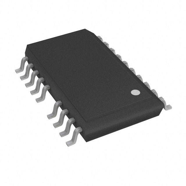
Infineon Technologies ICB2FL02GXUMA2
- Part No.:
- ICB2FL02GXUMA2
- Manufacturer:
- Infineon Technologies
- Category:
- Lighting, Ballast Controllers
- Package:
- 20-SOIC (0.295", 7.50mm Width), 19 Leads
- Datasheet:
-
 ICB2FL02GXUMA2.pdf
- Description:
- IC BALLAST CNTRL 120KHZ DSO-19
- Quantity:
- Payment:

- Shipping:

Inventory:3,196
Please send an inquiry. Send us your inquiry, and we will respond immediately.
Product details
Overview
ICB2FL02GXUMA2 from Infineon Technologies is a 2nd-generation smart ballast control IC for fluorescent lamp inverters, integrating discontinuous-mode PFC, high-voltage half-bridge driver (900 V), and digital timers up to 40 s. It supports T5/T8 single- and multi-lamp ballasts with current-mode preheating, EOL/rectifier-effect detection, and emergency lighting restart logic. Key confirmed parameters: 900 V half-bridge drive capability, ±25 mV/µs slope sensitivity at LSCS pin, 0.8 V overcurrent threshold, 500 ns fault latch delay, and RoHS-compliant PG-DSO-19-1 package.
For engineers reviewing the ICB2FL02GXUMA2 datasheet, ICB2FL02GXUMA2 pinout, ICB2FL02GXUMA2 application, or ICB2FL02GXUMA2 equivalent, this page delivers verified functional roles per pin, real-world protection behaviors (e.g., latched shutdown on >500 ns overcurrent), dimming-specific detection thresholds, and validated alternative controllers for fluorescent ballast redesigns - all grounded in Infineon's V1.2 preliminary datasheet and official package outline.
Technical Context
The ICB2FL02GXUMA2 implements a mixed-signal PFC architecture supporting DCM operation across 0–100% load range, with dedicated THD correction via ZCD signal and optional DCM-specific compensation. Its inverter section uses dual lamp voltage sense inputs (LVS1/LVS2) to distinguish open-filament HS vs. LS faults and detect capacitive-load operation below resonance.
Control timing is fully resistor-programmable: RFRUN sets run frequency, RFPH sets preheat frequency, and RTPH sets preheat duration. The IC features self-adapting dead time adjustment, clock-accelerated customer test mode, and latched fault handling triggered by monitored thresholds - not software polling.
Key Specifications
| Parameter | Value and Actual Design Meaning |
|---|---|
| PFC Mode | Discontinuous Conduction Mode (DCM) only; enables zero-current switching and low THD without requiring critical conduction mode circuitry. |
| Half-Bridge Drive Voltage | 900 V rated; supports direct driving of high-side MOSFETs in series-resonant fluorescent inverters without external level shifters. |
| LSCS Overcurrent Threshold | 0.8 V with 500 ns timeout; triggers latched shutdown to protect MOSFETs during short-circuit or end-of-life lamp failure. |
| Ignition Slope Sensitivity | 205 mV/µs ±25 mV/µs; enables precise filament warm-up control by detecting dI/dt during preheat phase. |
| Timer Range | Up to 40 seconds; digitally implemented with resistor-programmed accuracy stable over −25°C to +125°C ambient. |
| Dimming Thresholds | Dedicated analog comparators on LVS1/LVS2; detect lamp voltage asymmetry for analog dimming compatibility without external ADC. |
| Package | PG-DSO-19-1 (300 mil); 19-pin exposed-pad SOIC with creepage-enhanced layout for 2500 V RMS isolation compliance. |
Pinout & Package
ICB2FL02GXUMA2 is housed in a PG-DSO-19-1 (300 mil) package with integrated creepage distance enhancement and exposed thermal pad. Pin 16 is designated "Creepage distance" - a non-electrical mechanical feature, not a signal terminal.
| Pin/Terminal | Circuit Role | Design Meaning |
|---|---|---|
| 1 LSCS | Inverter low-side current sense | Direct shunt connection; internal 0.8 V comparator with 500 ns blanking for MOSFET overcurrent protection. |
| 2 LSGD | Inverter low-side gate driver | Capable of sinking 1 A peak; drives N-channel MOSFET source-connected to GND. |
| 3 VCC | Main supply input | Internal LDO input; powers core logic and gate drivers; requires external 15 V ±10% supply. |
| 4 GND | Low-side reference ground | Return path for LSCS, LSGD, and control logic; separate from HSGND to avoid noise coupling. |
| 5 PFCGD | PFC gate driver output | Drives PFC switch MOSFET gate; optimized for DCM switching transitions and low shoot-through risk. |
| 6 PFCCS | PFC current sense input | Connects to PFC inductor shunt; detects zero-current crossing and peak current for DCM regulation. |
| 7 PFCZCD | PFC zero-current detection | Input for auxiliary winding sensing; enables precise DCM boundary detection without secondary-side components. |
| 8 PFCVS | PFC bus voltage sense | Monitors bulk capacitor voltage; triggers OVP (95%) and UVP (75%) protection and open-loop detection. |
| 9 RFRUN | Run frequency programming | Resistor-to-ground sets inverter operating frequency during normal lamp operation (e.g., 40–80 kHz). |
| 10 RFPH | Preheat frequency programming | Resistor-to-ground sets lower-frequency preheat mode (e.g., 25–45 kHz) to limit filament stress. |
| 11 RTPH | Preheat time programming | Resistor-to-ground sets preheat duration (up to 40 s); determines thermal ramp before ignition. |
| 12 RES | Lamp removal restart enable | Pull-down to restart inverter after lamp replacement; avoids manual power cycle in maintenance scenarios. |
| 13 LVS1 | Lamp voltage sense 1 | High-side lamp terminal monitoring; used with LVS2 to detect asymmetric voltage collapse during EOL or rectifier effect. |
| 14 LVS2 | Lamp voltage sense 2 | Low-side lamp terminal monitoring; differential comparison with LVS1 enables capacitive-load detection. |
| 15 AUX | Auxiliary output | Open-drain output for status signaling (e.g., lamp-on indication or fault flag to MCU). |
| 17 HSGND | High-side floating ground | Reference for HSGD; tied to source of high-side MOSFET; isolated from main GND by bootstrap or transformer. |
| 18 HSVCC | High-side supply input | Bootstrap or transformer-derived supply for high-side driver; must be ≥10 V for reliable HSGD operation. |
| 19 HSGD | Inverter high-side gate driver | Level-shifted driver capable of 900 V blocking; sinks 0.5 A peak to drive high-side MOSFET gate. |
| 20 NC | No connect | Unbonded pin; must remain unconnected per datasheet; no internal circuitry attached. |
Key Features
| Feature | Design Value |
|---|---|
| Digital timer accuracy | ±2% over −25°C to +125°C; eliminates need for external RC timing networks and improves batch consistency. |
| Customer test mode | Hardware-enabled clock acceleration (via RTPH pin) reduces functional test time by >60% without firmware changes. |
| Emergency lighting restart | Skips preheat after brief line interruption (<200 ms), enabling seamless failover in battery-backed fixtures. |
| PFC THD optimization | Dedicated DCM-only compensation path reduces input current THD to <10% at full load without additional filtering. |
| Filament break detection | Separate thresholds for HS vs. LS filament opens during startup and run mode; prevents false ignitions and unsafe re-attempts. |
Applications
| Commercial T5/T8 Ballast | Emergency Lighting Fixture |
|---|---|
Use Scenario: 54 W T5 fluorescent fixture in office ceiling grid with 0–10 V dimming interface. IC Role / Device Role / Timing Role: Primary ballast controller managing PFC, preheat timing (RTPH), run frequency (RFRUN), and lamp voltage monitoring (LVS1/LVS2). Use Value: Enables single-chip implementation with <12 external passive components; meets EN61000-3-2 Class C THD limits without Y-capacitor oversizing. | Use Scenario: Battery-backed corridor light that must relight within 100 ms after AC loss. IC Role / Device Role / Timing Role: Fault-tolerant inverter controller using RES pin-triggered restart and skipped preheat logic during brownout recovery. Use Value: Eliminates need for external microcontroller supervision; achieves <50 ms lamp reignition time after AC restoration. |
| Multi-Lamp Industrial Ballast | Dimmable Architectural Lighting |
Use Scenario: 4×28 W T5 system in warehouse high-bay fixture with shared PFC stage. IC Role / Device Role / Timing Role: Master controller coordinating four parallel inverter legs via synchronized RFRUN/RFPH programming resistors. Use Value: Reduces component count by 30% vs. discrete ballast ICs; ensures identical preheat timing across all lamps for uniform aging. | Use Scenario: Museum display case with analog 1–10 V dimming and flicker-free low-end performance. IC Role / Device Role / Timing Role: Dimming-aware controller using LVS1/LVS2 differential sensing to maintain stable arc at 5% brightness. Use Value: Prevents lamp flicker and acoustic noise at 20–30 kHz dimming frequencies by adapting dead time and ignition thresholds. |
Equivalent & Alternatives
The following parts are listed as comparable options for similar fluorescent lamp ballast controller applications.
| Alternative Part | Technical Difference | Application Difference | Selection Advice |
|---|---|---|---|
| IRS2166DSPBF | Integrated bootstrap diode; lacks digital timers and customer test mode; analog-only PFC loop compensation. | Requires external RC timing network; no built-in lamp removal restart (RES) or clock acceleration. | Preferred for cost-sensitive, non-dimming single-lamp designs where test time reduction is not required. |
| UCC3305D | Fixed 65 kHz run frequency; no resistor-programmable preheat timing; no LVS1/LVS2 differential sensing. | Cannot support multi-lamp synchronization or EOL rectifier-effect detection; limited dimming adaptability. | Selected when legacy design reuse is prioritized and lamp voltage asymmetry monitoring is unnecessary. |
Compared with IRS2166DSPBF and UCC3305D, ICB2FL02GXUMA2 provides programmable timing, dual-lamp-voltage diagnostics, and hardware-accelerated testing - delivering higher reliability in commercial T5 systems and faster production validation without sacrificing analog control precision.
Availability
ICB2FL02GXUMA2 is available at Aetrix Electronics and suitable for commercial lighting ballasts, emergency lighting fixtures, industrial multi-lamp systems, and dimmable architectural installations requiring stable component supply and long-term lifecycle support.
Supply support for ICB2FL02GXUMA2 includes scheduled delivery planning, volume procurement assistance, BOM continuity management, traceable sourcing, and lifecycle availability coordination for OEM customers, industrial embedded developers, connected-device designers, and electronics production programs.
Manufacturer
Infineon Technologies AG is a German semiconductor manufacturer specializing in power management, automotive, and industrial control ICs, with global R&D and manufacturing infrastructure.
The ICB2FL02G belongs to Infineon's 2nd-generation fluorescent lamp controller product line, designed specifically for high-efficiency, low-THD electronic ballasts targeting T5/T8 lamp standards and emergency lighting compliance.
FAQ
What is the maximum allowable voltage on the HSGD pin?
The HSGD pin is rated for 900 V maximum blocking voltage, matching the IC's high-side driver specification. This rating is validated under continuous operation with proper PCB creepage (≥8 mm) and thermal management. Exceeding 900 V risks permanent damage to the level-shifting circuitry, and no transient overvoltage tolerance beyond this value is specified in the V1.2 datasheet.
Does ICB2FL02GXUMA2 support Power Factor Correction in Critical Conduction Mode (CRM)?
No - the ICB2FL02GXUMA2 supports only Discontinuous Conduction Mode (DCM) for PFC operation, as explicitly stated in Section 2.4.1 of the V1.2 datasheet. Its PFC control loop, ZCD detection, and THD correction features are architected exclusively for DCM; CRM operation is not implemented or characterized.
How is lamp end-of-life (EOL) detected using LVS1 and LVS2?
EOL detection uses differential comparison between LVS1 and LVS2: EOL1 (lamp overvoltage) triggers when LVS1 exceeds 320 V while LVS2 remains <100 V; EOL2 (rectifier effect) activates when both inputs show sustained asymmetry (>150 V difference) during run mode, indicating cathode degradation. These thresholds are fixed internal comparators, not resistor-programmable.
Can the customer test mode be activated without modifying hardware connections?
No - activation requires pulling the RTPH pin to GND (for preheat skip) or applying a specific voltage sequence to RTPH/RFPH pins (for clock acceleration), as defined in Sections 2.8.1 and 2.8.3. There is no register-based or I²C-accessible method; test mode is strictly hardware-controlled to ensure deterministic behavior during production testing.
ICB2FL02GXUMA2 Specifications
- Product attributes
- Attribute value
- Manufacturer:
- Infineon Technologies
- Series:
- -
- Package/Case:
- 20-SOIC (0.295", 7.50mm Width), 19 Leads
- Packaging:
- Tape & Reel (TR)
- Product Status:
- Obsolete
- Type:
- Ballast Controller
- Frequency:
- 20kHz ~ 120kHz
- Voltage - Supply:
- 10.6V ~ 17.5V
- Current - Supply:
- 4.2 mA
- Current - Output Source/Sink:
- -
- Dimming:
- No
- Operating Temperature:
- -25°C ~ 125°C
- Grade:
- -
- Qualification:
- -
- Mounting Type:
- Surface Mount
- Supplier Device Package:
- PG-DSO-19-1
ICB2FL02GXUMA2 FAQ
1.How can I place an order for ICB2FL02GXUMA2 through Aetrix?
Please submit a Request for Quotation (RFQ) for ICB2FL02GXUMA2 on Aetrix. Our sales agent will provide a competitive quotation and guide you through the order confirmation once you accept the terms.
2.Are the price and stock information for ICB2FL02GXUMA2 reliable?
The price and inventory of ICB2FL02GXUMA2 are updated periodically and may fluctuate due to market conditions. Stock and pricing data are typically refreshed every 24 hours. Quotation validity for ICB2FL02GXUMA2 is usually 5 days.
3.What payment methods are accepted for ICB2FL02GXUMA2?
We accept Wire Transfer, PayPal, Credit Card, Western Union, MoneyGram, and Escrow for ICB2FL02GXUMA2 transactions.
Note: Certain payment methods may incur a processing fee.
4.How is shipping managed for ICB2FL02GXUMA2?
ICB2FL02GXUMA2 orders can be shipped via leading logistics carriers, including DHL, UPS, FedEx, TNT, or Registered Mail.
Once your ICB2FL02GXUMA2 order is processed, you will receive an email with the shipment details and tracking number.
Note: Tracking information may take up to 24 hours to appear. Express delivery typically takes 3–5 business days.
5.How can I obtain technical support or documentation for ICB2FL02GXUMA2?
For technical support, including ICB2FL02GXUMA2 datasheets, pinout diagrams, or application guidance, please contact our engineering support team. They can provide detailed documentation and assistance for your ICB2FL02GXUMA2 requirements.
6.How does Aetrix verify that ICB2FL02GXUMA2 is sourced from the original manufacturer or authorized distributors?
All ICB2FL02GXUMA2 products on Aetrix are procured from qualified distributors and authorized channels. Our dedicated quality assurance team conducts strict verification, including traceability checks and, if necessary, third-party testing. This ensures that ICB2FL02GXUMA2 meets industry standards.
7.What is the process for return or replacement of ICB2FL02GXUMA2?
All ICB2FL02GXUMA2 units undergo pre-shipment inspection (PSI). If there is an issue with ICB2FL02GXUMA2, returns or replacements are accepted under the following conditions:
1.Quantity discrepancies, incorrect items, or visible external defects (such as breakage or corrosion), acknowledged by Aetrix.
2.The issue is reported within 90 days of delivery.
3.The ICB2FL02GXUMA2 part is unused and in its original packaging.
Return procedure for ICB2FL02GXUMA2:
1.Submit a request within 90 days.
2.Obtain a Return Material Authorization (RMA) from Aetrix.
ICB2FL02GXUMA2 Tags
-
HV833MG-G
Microchip Technology
-
HV857MG-G
Microchip Technology
-
MIC4826YMM-TR
Microchip Technology

-
HV823LG-G
Microchip Technology

-
IR2156STRPBF
Infineon Technologies
-
BTS712204ESAXUMA1
Infineon Technologies

-
UC3872DW
Texas Instruments
-
MAX14514ETD+
Analog Devices Inc./Maxim Integrated

-
MAX14521EETG+
Analog Devices Inc./Maxim Integrated
-
HV857LMG-G
Microchip Technology
-
HV860K7-G
Microchip Technology
-
MIC4832YMM
Microchip Technology
Tech Hub

Jumper cables guide covering safe connection order, red and black clamp placement, final ground connection, cable gauge, length, clamp quality, copper vs CCA cables, jump starter comparison and battery…

LDO regulator guide covering low dropout voltage, power dissipation, thermal design, PSRR, output noise, capacitor stability, adjustable LDO circuits, LDO vs buck converter and datasheet selection chec…

Conditional Access Module guide covering CAM meaning, CI/CI+ interface, smart card authorization, DVB security workflow, TV and set-top box compatibility, internal electronics, ESD protection, connecto…

Guide to electronic component obsolescence covering EOL risk, PCN/PDN notices, last-time buy planning, replacement options, form-fit-function validation, counterfeit risk and BOM lifecycle management.

18650 battery guide covering lithium-ion cell basics, 3.6V/3.7V voltage, 4.2V charging, mAh and Wh capacity, protected cells, chargers, BMS, series-parallel packs, holders, welding and sourcing checks.…

Hall effect sensor guide covering working principle, linear and digital sensors, Arduino circuits, current sensing, speed detection, automotive applications, A3144 examples, signal filtering and datash…

Product Change Notification guide for electronic components, covering PCN meaning, PCN vs PDN/EOL, common change types, risk levels, form-fit-function review, engineering validation, BOM control, LTB/L…

A practical guide to blend door actuators, covering HVAC function, symptoms, location, AC and heater issues, reset and calibration, replacement cost, electrical diagnosis, compatibility checks, and rep…

Engineering guide to Raspberry Pi alternatives, covering chip-level differences, Orange Pi, ROCK, Jetson, Banana Pi, NanoPi, Compute Module, Pico, GPIO, camera, HAT compatibility, and replacement risks…

Engineering guide to dynamic load response testing for high-current buck converters, covering load step setup, slew rate, Vcore undershoot, overshoot, recovery time, probe location, output capacitors a…


