
 My Inquiry
 My Account


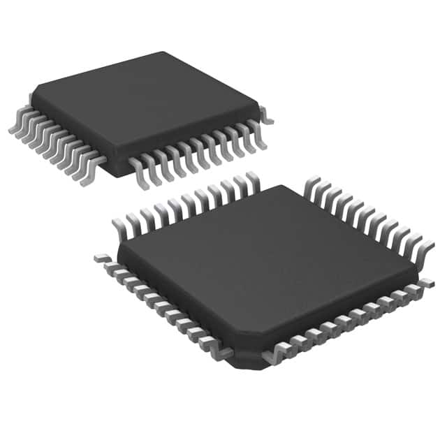
Renesas IDT728981DB
- Part No.:
- IDT728981DB
- Manufacturer:
- Renesas
- Category:
- Signal Switches, Multiplexers, Decoders
- Package:
- 44-QFP
- Datasheet:
-
 IDT728981DB.pdf
- Description:
- IC MULTIPLEXER 1 X 4:4 44PQFP
- Quantity:
- Payment:

- Shipping:

Inventory:3,568
Please send an inquiry. Send us your inquiry, and we will respond immediately.
Product details
Overview
IDT728981DB from Renesas Electronics (formerly IDT) is a 128×128 non-blocking time slot interchange (TSI) digital switch IC for ST-BUS®-compliant telecom systems. It supports four 2.048 Mb/s serial input streams (RX0–RX3), four 2.048 Mb/s serial output streams (TX0–TX3), microprocessor-controlled memory mapping, and operates at 5 V over –40°C to +85°C. It enables dynamic channel routing in PCM-based voice/data multiplexing equipment.
For engineers reviewing the IDT728981DB datasheet, IDT728981DB pinout, IDT728981DB application, or IDT728981DB equivalent, key selection criteria include ST-BUS® frame alignment timing (tFPS/tFPH), per-channel connection memory control (CMH/CML), ODE-driven three-state TX output management, and 44-pin PQFP package compatibility with legacy telecom backplane layouts.
Technical Context
The IDT728981DB implements dual-mode switching-Connection Mode (data routed via Data Memory using Connection Memory Low addresses) and Processor Mode (direct CML data output)-controlled by bit 6 (PE) of the Control Register. Its internal architecture includes on-chip serial-to-parallel and parallel-to-serial converters synchronized to a 4.096 MHz C4i clock and 8 kHz F0i frame pulse.
Channel addressing uses A0–A5 with Split Memory mode (SM bit) enabling simultaneous read-from-Data-Memory/write-to-Connection-Memory operations. Output drive state is managed hierarchically: ODE pin overrides all TX outputs globally, while individual CMH bit 0 (OE) and bit 2 (CS) enable per-channel three-state or source-selection control.
Key Specifications
| Parameter | Value and Actual Design Meaning |
|---|---|
| Switch Size | 128 × 128 non-blocking TSI matrix for full-time-slot reordering across 4 RX/4 TX streams |
| Serial Data Rate | 2.048 Mb/s per stream (32 × 64 Kbit/s channels), compliant with ETSI/G.704 ST-BUS® framing |
| Clock Input | C4i = 4.096 MHz - precisely twice frame rate; required for internal serial shift timing |
| Frame Sync | F0i = 8 kHz - defines 125 μs frames; used to reset internal address counter for channel framing |
| Supply Voltage | VCC = 4.75 V to 5.25 V - ensures TTL-compatible logic thresholds and stable memory operation |
| Operating Temp | –40°C to +85°C - qualified for industrial-grade telecom line cards and access concentrators |
| Micro Interface | 8-bit parallel bus (D0–D7), A0–A5, CS, DS, R/W - supports standard 80Cxx/68K-style processor access |
Pinout & Package
Package: 44-pin Plastic Quad Flatpack (PQFP), 10 mm × 10 mm, 0.80 mm pitch (order code DB). Pin 1 index corner marked; pins 1–22 and 33–44 on top/bottom edges, pins 23–32 on right edge.
| Pin/Terminal | Circuit Role | Design Meaning |
|---|---|---|
| GND (Pins 11, 22) | Ground reference | Dual ground pins reduce noise coupling between analog timing and digital I/O sections |
| VCC (Pins 21, 23, 24, 25) | +5 V supply | Four dedicated VCC pins ensure low-impedance power delivery to internal memory and I/O drivers |
| RX0–RX3 (Pins 39–42) | Serial input streams | Accept continuous 2.048 Mb/s ST-BUS® frames; each carries 32 × 8-bit PCM channels |
| TX0–TX3 (Pins 1–4) | Three-state serial outputs | Output re-routed time slots; high-impedance when ODE = LOW or CMH.OE = 0 |
| ODE (Pin 5) | Global output enable | Master control: LOW forces all TX0–TX3 into high-Z regardless of CMH settings |
| F0i (Pin 37) | 8 kHz frame sync input | Resets internal counter to align channel addressing with ST-BUS® frame boundaries |
| C4i (Pin 38) | 4.096 MHz serial clock | Drives internal shift registers; determines minimum tCLK = 220 ns timing constraint |
| A0–A5 (Pins 12, 13, 15–17, 20) | Address inputs | Select Control Register (A5=0) or 32-channel memory block (A5=1); define stream subsection via STA bits |
| D0–D7 (Pins 10, 18, 19, 26–31) | Bi-directional data bus | Read/write access to Control Register, Data Memory, Connection Memory HIGH/LOW |
| DTA (Pin 6) | Data acknowledge | Open-drain active-LOW pulse confirms completion of microprocessor bus transaction |
Key Features
| Feature | Design Value |
|---|---|
| ST-BUS® Compliance | Fully compatible with Mitel's ST-BUS® physical layer: 2.048 Mb/s, 125 μs frames, 32-channel structure |
| Dual Switching Modes | Hardware-selectable Connection Mode (memory-mapped routing) or Processor Mode (direct CML output) |
| Hierarchical Output Control | ODE pin provides system-level three-state override; CMH.OE enables per-channel driver gating |
| Split Memory Access | SM bit allows concurrent read-from-Data-Memory and write-to-Connection-Memory in single bus cycle |
| Power-Up Safety | ODE must be held LOW at startup to prevent bus contention until CMH is initialized |
Applications
| PCM Multiplexer | Digital Loop Carrier |
|---|---|
Use Scenario: Aggregating 128 subscriber lines into E1/T1 trunks with dynamic time-slot assignment. IC Role / Device Role / Timing Role: Time slot interchange core performing real-time PCM sample reordering under microprocessor control. Use Value: Enables flexible circuit-switched voice path allocation without external RAM or FPGA glue logic. | Use Scenario: Remote terminal unit in DSLAM or fiber node handling multiple T1/E1 interfaces. IC Role / Device Role / Timing Role: Central TSI fabric interconnecting line interface units (LIUs) and concentrator processors. Use Value: Supports hot-swappable LIU modules via ODE-controlled TX isolation and per-channel OE masking. |
| ISDN PRI Gateway | VoIP Media Gateway |
Use Scenario: Bridging 30 B-channels between ISDN PRI and IP-based softswitch infrastructure. IC Role / Device Role / Timing Role: ST-BUS®-to-PCI bridge element converting synchronous TDM to packetized media streams. Use Value: Provides deterministic 2-channel minimum delay (per Table 1) for low-jitter voice path stitching. | Use Scenario: Legacy PBX integration where analog/digital trunk lines feed VoIP gateways. IC Role / Device Role / Timing Role: TDM switch fabric enabling selective grooming of voice channels before DSP processing. Use Value: Allows software-defined channel mapping (via CML writes) to match codec resource allocation. |
Equivalent & Alternatives
The following parts are listed as comparable options for similar time slot interchange applications.
| Alternative Part | Technical Difference | Application Difference | Selection Advice |
|---|---|---|---|
| MC145506P | 80×80 TSI, single 2.048 Mb/s bidirectional port, no microprocessor interface | Limited to smaller-scale concentrators; requires external logic for multi-port expansion | Choose when board space is constrained and switching density < 100 channels suffices |
| Si2404-GM | 128×128 TSI, integrated PLL, 3.3 V operation, QFN-64 package | Requires level-shifting for 5 V ST-BUS® interface; lacks ODE pin for global TX disable | Prefer for new designs targeting lower power and higher integration, but verify F0i/C4i timing compatibility |
Compared with MC145506P and Si2404-GM, the IDT728981DB uniquely combines full 128×128 non-blocking capacity, native 5 V ST-BUS® compliance, hierarchical ODE/CMH output control, and 44-pin PQFP footprint-making it optimal for drop-in replacement in legacy telecom hardware requiring field-proven reliability and minimal layout change.
Availability
IDT728981DB is available at Aetrix Electronics and suitable for PCM multiplexers, digital loop carriers, ISDN PRI gateways, and VoIP media gateways requiring stable component supply across extended product lifecycles.
Supply support for IDT728981DB includes scheduled delivery planning, volume procurement assistance, BOM continuity management, traceable sourcing, and lifecycle availability coordination for OEM customers, industrial embedded developers, connected-device designers, and electronics production programs.
Manufacturer
Renesas Electronics Corporation is a global semiconductor leader specializing in microcontrollers, analog, power, and connectivity solutions for automotive, industrial, and infrastructure markets.
The IDT728981DB belongs to Renesas' legacy IDT telecom timing and switching portfolio, designed specifically for carrier-grade TDM infrastructure requiring deterministic time-slot routing, ST-BUS® interoperability, and long-term industrial temperature operation.
FAQ
What is the primary function of the IDT728981DB in a telecom system?
The IDT728981DB serves as a 128×128 non-blocking time slot interchange digital switch that dynamically routes PCM voice/data channels between four 2.048 Mb/s ST-BUS® input and output streams. It enables real-time reordering of time slots under microprocessor control, supporting applications like PCM multiplexing and ISDN PRI gatewaying. Its dual-mode operation (Connection Mode and Processor Mode) and hierarchical output control make the IDT728981DB especially suited for flexible, software-configurable TDM switching fabrics.
How does the ODE pin affect the behavior of the IDT728981DB TX outputs?
The ODE (Output Drive Enable) pin is a master three-state control for all TX0–TX3 serial outputs. When ODE is held LOW, all TX outputs are forced into high-impedance state regardless of Connection Memory High (CMH) settings-this prevents bus contention during power-up or fault conditions. When ODE is HIGH, individual TX channel drivers are enabled or disabled based on CMH bit 0 (OE). This two-tier control makes the IDT728981DB robust for hot-swap and fail-safe telecom designs.
What timing constraints govern the IDT728981DB's frame synchronization interface?
The IDT728981DB requires precise 8 kHz F0i frame pulse and 4.096 MHz C4i clock inputs. Key AC parameters include F0i setup time (tFPS ≥ 20 ns), hold time (tFPH ≥ 0.020 μs), and pulse width (tFPW ≈ 244 ns), all referenced to C4i edges. These ensure correct alignment of the internal 125 μs frame counter and accurate channel addressing. Violating tFPS or tFPH risks misframing and data corruption-designs must route F0i with matched trace length to C4i. The IDT728981DB datasheet specifies these values under recommended operating conditions.
Can the IDT728981DB operate in both Connection Mode and Processor Mode simultaneously?
No-the IDT728981DB operates exclusively in one mode at a time, selected by bit 6 (PE) of the Control Register. When PE = 1, all TX channels output Connection Memory Low (CML) contents-Processor Mode. When PE = 0, each channel's behavior is determined individually by CMH bit 2 (CS): CS = 1 selects Processor Mode for that channel; CS = 0 selects Connection Mode (routing via Data Memory address). Thus, mixed-mode operation is possible per channel, but global mode selection is binary. This flexibility is documented in Table 3 and Figure 2 of the IDT728981DB functional description.
What package type does the IDT728981DB use, and why is it significant for telecom PCB design?
The IDT728981DB uses a 44-pin Plastic Quad Flatpack (PQFP), 10 mm × 10 mm, 0.80 mm pitch (order code DB). This package maintains pin compatibility with legacy IDT728981 variants in PLCC (J) and PDIP (P) packages, enabling drop-in replacement in existing telecom line cards. Its gull-wing leads support automated optical inspection and reflow soldering, while the 44-pin count accommodates all critical signals-including four RX/TX pairs, 8-bit data bus, six address lines, and dedicated control pins-without requiring interposer boards. This makes the IDT728981DB ideal for cost-sensitive, high-reliability telecom upgrades.
IDT728981DB Specifications
- Product attributes
- Attribute value
- Manufacturer:
- Renesas
- Series:
- 7200
- Package/Case:
- 44-QFP
- Packaging:
- Tube
- Product Status:
- Obsolete
- Type:
- Multiplexer
- Circuit:
- 1 x 4:4
- Independent Circuits:
- 1
- Current - Output High, Low:
- -
- Voltage Supply Source:
- Single Supply
- Voltage - Supply:
- 4.75V ~ 5.25V
- Operating Temperature:
- -40°C ~ 85°C
- Grade:
- -
- Qualification:
- -
- Mounting Type:
- Surface Mount
- Supplier Device Package:
- 44-PQFP (10x10)
IDT728981DB FAQ
1.How can I place an order for IDT728981DB through Aetrix?
Please submit a Request for Quotation (RFQ) for IDT728981DB on Aetrix. Our sales agent will provide a competitive quotation and guide you through the order confirmation once you accept the terms.
2.Are the price and stock information for IDT728981DB reliable?
The price and inventory of IDT728981DB are updated periodically and may fluctuate due to market conditions. Stock and pricing data are typically refreshed every 24 hours. Quotation validity for IDT728981DB is usually 5 days.
3.What payment methods are accepted for IDT728981DB?
We accept Wire Transfer, PayPal, Credit Card, Western Union, MoneyGram, and Escrow for IDT728981DB transactions.
Note: Certain payment methods may incur a processing fee.
4.How is shipping managed for IDT728981DB?
IDT728981DB orders can be shipped via leading logistics carriers, including DHL, UPS, FedEx, TNT, or Registered Mail.
Once your IDT728981DB order is processed, you will receive an email with the shipment details and tracking number.
Note: Tracking information may take up to 24 hours to appear. Express delivery typically takes 3–5 business days.
5.How can I obtain technical support or documentation for IDT728981DB?
For technical support, including IDT728981DB datasheets, pinout diagrams, or application guidance, please contact our engineering support team. They can provide detailed documentation and assistance for your IDT728981DB requirements.
6.How does Aetrix verify that IDT728981DB is sourced from the original manufacturer or authorized distributors?
All IDT728981DB products on Aetrix are procured from qualified distributors and authorized channels. Our dedicated quality assurance team conducts strict verification, including traceability checks and, if necessary, third-party testing. This ensures that IDT728981DB meets industry standards.
7.What is the process for return or replacement of IDT728981DB?
All IDT728981DB units undergo pre-shipment inspection (PSI). If there is an issue with IDT728981DB, returns or replacements are accepted under the following conditions:
1.Quantity discrepancies, incorrect items, or visible external defects (such as breakage or corrosion), acknowledged by Aetrix.
2.The issue is reported within 90 days of delivery.
3.The IDT728981DB part is unused and in its original packaging.
Return procedure for IDT728981DB:
1.Submit a request within 90 days.
2.Obtain a Return Material Authorization (RMA) from Aetrix.
IDT728981DB Tags

-
SN74HC138DR
Texas Instruments
-
TC7SB3157CFU,LF(CT
Toshiba Semiconductor and Storage
-
74CBTLV3257PW,118
Nexperia USA Inc.

-
SN74CBTLV3257PWR
Texas Instruments
-
74CBTLV3257GUX
Nexperia USA Inc.
-
74HC154BQ,118
Nexperia USA Inc.

-
P3S0200GMX
NXP USA Inc.

-
SN74CB3Q3245PWR
Texas Instruments
-
SN74CB3Q3257RGYR
Texas Instruments

-
TCA9543APWR
Texas Instruments
-
TCA9546APWR
Texas Instruments

-
SN74HC138N
Texas Instruments
Tech Hub

TTL and CMOS logic families differ in thresholds, loading, output drive, power and timing. This engineering guide compares 74HC and 74HCT, calculates noise margins and checks 3.3 V/5 V compatibility.

A practical engineering guide to 3.3V and 5V logic compatibility, input thresholds, resistor dividers, translator ICs, MOSFET level shifting, I2C pull-ups, timing limits and power-sequencing risks.

The 74HC595 uses push-pull logic outputs, while the TPIC6B595 uses 50 V open-drain DMOS sinks for higher-power loads. This guide compares timing, current limits, 3.3 V interfacing, load wiring, thermal…

The 74HC595 converts serial data into eight stable parallel outputs. This guide covers pin functions, shift and storage timing, OE and MR behavior, drive-current limits, cascading, voltage compatibilit…

A technical comparison of level-sensitive latches and edge-triggered flip-flops, covering timing windows, setup and hold limits, master–slave operation, time borrowing, race-through, HDL inference and…

A D latch stores one bit while Enable controls when data can pass. This reference covers gate-level operation, truth tables, transparency, setup and hold timing, LE versus OE, common ICs and practical …

An SR latch stores one bit through cross-coupled feedback. This engineering reference covers NOR and NAND implementations, truth tables, forbidden-state recovery, gated operation, switch debouncing, fa…

Latch circuits retain one bit through feedback. This technical reference covers SR and D latches, truth tables, transparency, timing limits, latch-versus-flip-flop behavior, applications and common log…

An engineering guide to LED driver operation, constant-current and constant-voltage outputs, linear and switching topologies, dimming, IC selection, calculations, replacement compatibility, and fault c…

Operational amplifier guide covering op amp basics, feedback, ideal vs real op amps, common configurations, buffer circuits, offset, bias current, gain-bandwidth, slew rate, rail-to-rail limits and sel…


