
 My Inquiry
 My Account


Renesas IDT79R3041-33PF
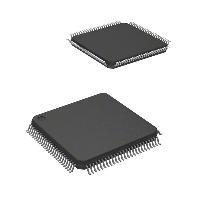
- Part No.:
- IDT79R3041-33PF
- Manufacturer:
- Renesas
- Category:
- Microprocessors
- Package:
- 100-LQFP
- Datasheet:
-
 IDT79R3041-33PF.pdf
- Description:
- IC MPU 33MHZ 100TQFP
- Quantity:
- Payment:

- Shipping:

Inventory:4,475
Please send an inquiry. Send us your inquiry, and we will respond immediately.
Product details
Overview
IDT79R3041-33PF from Integrated Device Technology is a 32-bit MIPS RISC microprocessor with integrated instruction cache (2 kB), data cache (512 B), programmable bus interface, on-chip DMA arbiter, and 24-bit timer. It operates at 33 MHz, delivers 20 MIPS at 25 MHz, and supports 8-/16-/32-bit memory port widths. Designed for cost-sensitive embedded systems such as laser printer controllers and PDL interpreters.
For engineers reviewing the IDT79R3041-33PF datasheet, IDT79R3041-33PF pinout, IDT79R3041-33PF application, or IDT79R3041-33PF equivalent, key selection criteria include its PLCC-84 package, double-frequency clock input (ClkIn), SysClk output timing feedback, and software compatibility with the IDT79R3000A and broader RISController family.
Technical Context
The IDT79R3041-33PF implements the MIPS-I ISA with a five-stage pipeline and 32 orthogonal 32-bit general-purpose registers. Its CPU core is binary-compatible with the IDT79R3000A, enabling direct software reuse without recompilation.
It integrates a System Control Coprocessor (CP0) managing exception handling, virtual-to-physical address mapping (base architecture, no TLB), cache configuration, bus timing control, and programmable port width per physical address sub-region - all configurable via CP0 registers at reset or runtime.
Key Specifications
| Parameter | Value and Actual Design Meaning |
|---|---|
| Clock Input | Double-frequency ClkIn (e.g., 66 MHz for 33 MHz core operation); eliminates external delay line required by R3000A designs. |
| Core Frequency | 33 MHz maximum rated operation; achieves 20 MIPS at 25 MHz when executing from cache. |
| Instruction Cache | 2 kB direct-mapped physical-address cache with 16-byte line size; avoids context-switch flushes and enables high hit rates from low-cost memory. |
| Data Cache | 512 B direct-mapped write-through physical-address cache; paired with 4-deep write buffer to eliminate memory-write stalls. |
| Bus Interface | 32-bit multiplexed address/data bus with ALE, Rd/Wr, DataEn, MemStrobe; supports programmable 8-/16-/32-bit port widths and extended address hold timing. |
| On-chip Peripherals | 4-deep read/write buffers, DMA arbiter, 24-bit programmable timer (Count/Compare registers), and boot-from-PROM capability across all port widths. |
| Memory Mapping | 4 GB physical address space with kseg0/kseg1/kuseg segmentation; no TLB - uses simple address decoding for kernel/user protection. |
Pinout & Package
Package: 84-pin Plastic Leaded Chip Carrier (PLCC), cavity-down, commercial temperature range (0°C to +85°C).
| Pin/Terminal | Circuit Role | Design Meaning |
|---|---|---|
| A/D(31:0) | Time-multiplexed address/data bus | Carries 32-bit address in first phase (latched by ALE), then 32-bit data; supports byte-enable (BE16) and burst/wr-near modes. |
| ClkIn | Primary clock input | Accepts double-frequency signal (e.g., 66 MHz); internal clock generator derives core and SysClk signals with precise phase alignment. |
| SysClk | System clock output | Feedback-referenced clock used by external logic to meet tight setup/hold timing; drives ALE and bus control with minimal skew. |
| ALE | Address Latch Enable | Indicates valid address phase on A/D bus; internal feedback ensures adequate address hold time for low-cost latches/FPGAs. |
| Reset | Active-low asynchronous reset | Samples Reset Configuration Mode inputs (e.g., endian mode, cache refill size) on assertion; initializes CP0 registers and pipeline state. |
| Int(5:3), SInt(2:0) | Interrupt request inputs | Seven-level prioritized interrupt system supporting both maskable (Int) and software-triggered (SInt) events for real-time response. |
| TC | Timer Count output | 24-bit timer output usable for DRAM refresh or general-purpose timing; controlled via CP0 Count/Compare registers. |
Key Features
| Feature | Design Value |
|---|---|
| Programmable port width per memory region | Kernel software configures 8-/16-/32-bit port widths independently per physical address sub-region - enables mixed-width systems (e.g., 8-bit PROM + 32-bit DRAM) without external packing logic. |
| Extended Address Hold mode | Adds ½ clock cycle of address hold after ALE falling edge - allows use of slower, lower-cost address latches, FPGAs, and ASICs without timing violations. |
| 4-deep write buffer | Decouples CPU store execution rate from memory write speed - prevents pipeline stalls during writes to slow memory or narrow ports. |
| 4-deep read buffer | Queues burst-read data internally before cache fill - enables page-mode or static-column DRAM usage while sustaining high effective bandwidth. |
| Big/Little Endian runtime switch | Configurable at reset or dynamically via CP0 - simplifies porting legacy code and interoperability with heterogeneous processor systems or databases. |
Applications
| Laser Printer Controller | PostScript Interpreter System |
|---|---|
Use Scenario: Embedded controller managing print engine timing, raster image processing, and font rendering in mid-volume laser printers. IC Role / Device Role / Timing Role: Primary RISC CPU executing Adobe PostScript PDL interpreter firmware; coordinates DRAM frame buffer, I/O peripherals, and laser engine interface. Use Value: Programmable 16-bit DRAM interface and 8-bit boot PROM support reduce BOM cost; 2 kB instruction cache enables fast PDL bytecode execution from low-speed EPROM. | Use Scenario: Standalone PDL interpreter board running Adobe PostScript or Microsoft TrueImage in networked document systems. IC Role / Device Role / Timing Role: Host processor managing cartridge-based font loading, scalable graphics rendering, and bidirectional LAN/RS-422 communication. Use Value: 32-bit PROM interface handles large PDL interpreter binaries; 4-deep read buffer sustains burst reads from page-mode DRAM for high-resolution rasterization. |
| Field-Upgradeable Embedded System | Low-Cost Industrial HMI |
Use Scenario: Modular industrial controller where memory subsystems (e.g., frame buffer, firmware storage) are upgraded in-field without PCB redesign. IC Role / Device Role / Timing Role: Core processor maintaining software compatibility across memory upgrades (e.g., 16-bit → 32-bit DRAM) via transparent data packing/unpacking. Use Value: Port width programmability and on-chip data packing allow same firmware to run unchanged across hardware revisions - eliminating requalification effort. | Use Scenario: Human-machine interface panel with RS-232/422 serial comms, local display buffer, and keypad scanning in factory automation. IC Role / Device Role / Timing Role: Real-time controller managing concurrent I/O polling, display refresh, and protocol stack execution with deterministic latency. Use Value: 24-bit timer provides precise DRAM refresh and UI timing; 7-level interrupt system guarantees responsive button/key event handling. |
Equivalent & Alternatives
The following parts are listed as comparable options for similar RISC microprocessor applications.
| Alternative Part | Technical Difference | Application Difference | Selection Advice |
|---|---|---|---|
| IDT79R3051-33PF | 4 kB instruction cache, 2 kB data cache, optional MMU/TLB; same PLCC-84 package and pinout. | Supports full virtual memory and protected OS environments; requires TLB-aware software. | Select when migrating from IDT79R3041-33PF to enable multitasking OS or memory protection without PCB change. |
| IDT79R3081-33PF | Hardware floating-point unit, larger caches (up to 8 kB/8 kB), higher power envelope; same pinout but MQUAD package option. | Targeted at compute-intensive embedded applications requiring IEEE-754 FP math (e.g., motion control, signal analysis). | Choose only if floating-point performance is mandatory; not drop-in due to thermal and power delivery differences despite pin compatibility. |
Compared with IDT79R3041-33PF, IDT79R3051-33PF adds MMU support for secure multitasking but increases software complexity, while IDT79R3081-33PF delivers hardware FP acceleration at the cost of higher power and thermal management requirements - neither replaces IDT79R3041-33PF in cost-optimized, cache-driven embedded control roles.
Availability
IDT79R3041-33PF is available at Aetrix Electronics and suitable for laser printer controllers, PostScript interpreter systems, field-upgradeable embedded platforms, low-cost industrial HMIs, and PDL-based document processing requiring stable component supply over extended production lifecycles.
Supply support for IDT79R3041-33PF includes scheduled delivery planning, volume procurement assistance, BOM continuity management, traceable sourcing, and lifecycle availability coordination for OEM customers, industrial embedded developers, connected-device designers, and electronics production programs.
Manufacturer
Integrated Device Technology, Inc. (IDT) was a fabless semiconductor company specializing in high-performance timing, memory interface, and embedded processor solutions before its acquisition by Renesas Electronics in 2019.
The RISController family - including IDT79R3041-33PF - was designed to deliver MIPS RISC performance in cost-sensitive embedded applications like laser printing, PDL interpretation, and industrial control, emphasizing integration, power efficiency, and mixed-width memory interfacing.
FAQ
What is the maximum operating frequency of the IDT79R3041-33PF?
The IDT79R3041-33PF is rated for 33 MHz operation, with its double-frequency ClkIn input requiring a 66 MHz signal. It achieves 20 MIPS performance at 25 MHz when executing from its on-chip instruction cache. The "33" in the part number explicitly denotes this 33 MHz maximum rating under commercial temperature conditions (0°C to +85°C).
Does the IDT79R3041-33PF include a memory management unit (MMU)?
No, the IDT79R3041-33PF does not include an MMU or TLB. It implements the base RISController architecture with fixed virtual-to-physical address mapping (kseg0/kseg1/kuseg segmentation) and relies on external address decoding for memory protection. This simplifies software and reduces cost compared to MMU-equipped variants like the IDT79R3051-33PF.
How does the IDT79R3041-33PF support mixed-width memory systems?
The IDT79R3041-33PF supports 8-, 16-, and 32-bit memory port widths via its Port Size Control Register in CP0. Kernel software can assign different widths to distinct physical address sub-regions, enabling simultaneous use of an 8-bit boot PROM, 16-bit font cartridge, and 32-bit main DRAM - all with transparent on-chip data packing/unpacking and no external logic.
What is the function of the SysClk pin on the IDT79R3041-33PF?
The SysClk pin on the IDT79R3041-33PF outputs a feedback-referenced system clock derived from ClkIn. It is used by external logic (e.g., address latches, transceivers) to meet precise setup/hold timing relative to the CPU's internal bus interface - reducing skew and enabling reliable interfacing with low-cost components without complex PCB layout constraints.
Can the IDT79R3041-33PF execute code directly from external ROM without caching?
Yes, the IDT79R3041-33PF can execute code directly from external ROM using uncached accesses. Its instruction cache is optional and can be disabled via CP0 configuration. However, performance drops significantly without caching - the 2 kB instruction cache is essential to achieving 20 MIPS at 25 MHz, especially when sourcing from low-speed EPROM or flash devices.
IDT79R3041-33PF Specifications
- Product attributes
- Attribute value
- Manufacturer:
- Renesas
- Package/Case:
- 100-LQFP
- Series:
- -
- Packaging:
- Tray
- Product Status:
- Obsolete
- Core Processor:
- MIPS-I
- Number of Cores/Bus Width:
- 1 Core, 32-Bit
- Speed:
- 33MHz
- Co-Processors/DSP:
- System Control; CP0
- RAM Controllers:
- DRAM
- Graphics Acceleration:
- No
- Display & Interface Controllers:
- -
- Ethernet:
- -
- SATA:
- -
- USB:
- -
- Voltage - I/O:
- 5.0V
- Operating Temperature:
- 0°C ~ 85°C (TC)
- Grade:
- -
- Qualification:
- -
- Security Features:
- -
- Mounting Type:
- Surface Mount
- Supplier Device Package:
- 100-TQFP (14x14)
- Additional Interfaces:
- -
IDT79R3041-33PF FAQ
1.How can I place an order for IDT79R3041-33PF through Aetrix?
Please submit a Request for Quotation (RFQ) for IDT79R3041-33PF on Aetrix. Our sales agent will provide a competitive quotation and guide you through the order confirmation once you accept the terms.
2.Are the price and stock information for IDT79R3041-33PF reliable?
The price and inventory of IDT79R3041-33PF are updated periodically and may fluctuate due to market conditions. Stock and pricing data are typically refreshed every 24 hours. Quotation validity for IDT79R3041-33PF is usually 5 days.
3.What payment methods are accepted for IDT79R3041-33PF?
We accept Wire Transfer, PayPal, Credit Card, Western Union, MoneyGram, and Escrow for IDT79R3041-33PF transactions.
Note: Certain payment methods may incur a processing fee.
4.How is shipping managed for IDT79R3041-33PF?
IDT79R3041-33PF orders can be shipped via leading logistics carriers, including DHL, UPS, FedEx, TNT, or Registered Mail.
Once your IDT79R3041-33PF order is processed, you will receive an email with the shipment details and tracking number.
Note: Tracking information may take up to 24 hours to appear. Express delivery typically takes 3–5 business days.
5.How can I obtain technical support or documentation for IDT79R3041-33PF?
For technical support, including IDT79R3041-33PF datasheets, pinout diagrams, or application guidance, please contact our engineering support team. They can provide detailed documentation and assistance for your IDT79R3041-33PF requirements.
6.How does Aetrix verify that IDT79R3041-33PF is sourced from the original manufacturer or authorized distributors?
All IDT79R3041-33PF products on Aetrix are procured from qualified distributors and authorized channels. Our dedicated quality assurance team conducts strict verification, including traceability checks and, if necessary, third-party testing. This ensures that IDT79R3041-33PF meets industry standards.
7.What is the process for return or replacement of IDT79R3041-33PF?
All IDT79R3041-33PF units undergo pre-shipment inspection (PSI). If there is an issue with IDT79R3041-33PF, returns or replacements are accepted under the following conditions:
1.Quantity discrepancies, incorrect items, or visible external defects (such as breakage or corrosion), acknowledged by Aetrix.
2.The issue is reported within 90 days of delivery.
3.The IDT79R3041-33PF part is unused and in its original packaging.
Return procedure for IDT79R3041-33PF:
1.Submit a request within 90 days.
2.Obtain a Return Material Authorization (RMA) from Aetrix.
IDT79R3041-33PF Tags

-
AT91SAM9260B-CU-999
Microchip Technology
-
AT91SAM9G25-CU
Microchip Technology

-
ATSAMA5D27C-CU
Microchip Technology
-
AT91SAM9X35-CU
Microchip Technology
-
AT91SAM9X25-CU
Microchip Technology

-
MCIMX6Y2CVM08AB
NXP Semiconductors
.JPG)
-
AM3352BZCZ100
Texas Instruments
-
AT91SAM9260B-CU
Microchip Technology

-
AT91SAM9260B-QU
Microchip Technology

-
ATSAMA5D31A-CU
Microchip Technology
-
AT91SAM9G20B-CU-999
Microchip Technology
-
MCIMX6Y2CVM05AB
NXP Semiconductors
Tech Hub

A practical engineering and sourcing framework covering lifecycle verification, lifetime-buy calculations, replacement qualification, supplier checks and counterfeit-risk controls.

TTL and CMOS logic families differ in thresholds, loading, output drive, power and timing. This engineering guide compares 74HC and 74HCT, calculates noise margins and checks 3.3 V/5 V compatibility.

A practical engineering guide to 3.3V and 5V logic compatibility, input thresholds, resistor dividers, translator ICs, MOSFET level shifting, I2C pull-ups, timing limits and power-sequencing risks.

The 74HC595 uses push-pull logic outputs, while the TPIC6B595 uses 50 V open-drain DMOS sinks for higher-power loads. This guide compares timing, current limits, 3.3 V interfacing, load wiring, thermal…

The 74HC595 converts serial data into eight stable parallel outputs. This guide covers pin functions, shift and storage timing, OE and MR behavior, drive-current limits, cascading, voltage compatibilit…

A technical comparison of level-sensitive latches and edge-triggered flip-flops, covering timing windows, setup and hold limits, master–slave operation, time borrowing, race-through, HDL inference and…

A D latch stores one bit while Enable controls when data can pass. This reference covers gate-level operation, truth tables, transparency, setup and hold timing, LE versus OE, common ICs and practical …

An SR latch stores one bit through cross-coupled feedback. This engineering reference covers NOR and NAND implementations, truth tables, forbidden-state recovery, gated operation, switch debouncing, fa…

Latch circuits retain one bit through feedback. This technical reference covers SR and D latches, truth tables, transparency, timing limits, latch-versus-flip-flop behavior, applications and common log…

An engineering guide to LED driver operation, constant-current and constant-voltage outputs, linear and switching topologies, dimming, IC selection, calculations, replacement compatibility, and fault c…


