
 My Inquiry
 My Account


Renesas IDT79R3041-33PFG
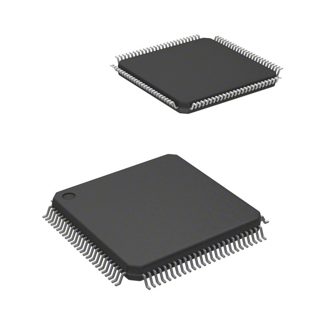
- Part No.:
- IDT79R3041-33PFG
- Manufacturer:
- Renesas
- Category:
- Microprocessors
- Package:
- 100-LQFP
- Datasheet:
-
 IDT79R3041-33PFG.pdf
- Description:
- IC MPU 33MHZ 100TQFP
- Quantity:
- Payment:

- Shipping:

Inventory:1,063
Please send an inquiry. Send us your inquiry, and we will respond immediately.
Product details
Overview
IDT79R3041-33PFG from Integrated Device Technology is a 32-bit MIPS RISC microprocessor with integrated instruction cache (2 kB), data cache (512 B), programmable bus interface, on-chip DMA arbiter, and 24-bit timer. It operates at 33 MHz, delivers 20 MIPS at 25 MHz, supports 8-/16-/32-bit memory port widths, and targets cost-sensitive embedded systems such as laser printer controllers and low-cost network peripherals.
For engineers reviewing the IDT79R3041-33PFG datasheet, IDT79R3041-33PFG pinout, IDT79R3041-33PFG application, or IDT79R3041-33PFG equivalent, key selection criteria include its PLCC-84 package, double-frequency clock input (ClkIn), SysClk output timing feedback, A/D(31:0) multiplexed address/data bus, and software compatibility with the IDT RISController family including R3000A and R3081.
Technical Context
The IDT79R3041-33PFG implements the MIPS-I ISA with a five-stage pipeline and 32 orthogonal 32-bit general-purpose registers. Its CPU core is binary-compatible with the IDT79R3000A, enabling reuse of existing MIPS toolchains and firmware.
It integrates a System Control Coprocessor (CP0) managing exception handling, virtual-to-physical address mapping without TLB, cache configuration, bus timing control, and programmable port width per memory sub-region. The bus interface supports burst reads via a 4-deep read buffer and eliminates write stalls using a 4-deep write buffer.
Key Specifications
| Parameter | Value and Actual Design Meaning |
|---|---|
| Clock Input | Double-frequency ClkIn (66 MHz nominal for 33 MHz core operation); enables internal clock generation without external delay lines |
| Core Frequency | 33 MHz maximum operation; achieves 20 MIPS at 25 MHz when executing from cache |
| Instruction Cache | 2 kB direct-mapped physical-address cache with 16-byte line size; eliminates instruction fetch stalls from slow memory |
| Data Cache | 512 B direct-mapped write-through physical-address cache; ensures main memory coherency without software intervention |
| Bus Interface | 32-bit multiplexed address/data bus (A/D31:0) with ALE, Rd, Wr, DataEn, and programmable timing (e.g., extended address hold) |
| Memory Port Width | Software-configurable 8-, 16-, or 32-bit port support per physical address sub-region; enables mixed-width memory systems without external packing logic |
| On-chip Peripherals | 24-bit programmable timer (Count/Compare registers), DMA arbiter, and boot-from-PROM capability for 8/16/32-bit PROMs |
Pinout & Package
Package: 84-pin Plastic Leaded Chip Carrier (PLCC), cavity-down, commercial temperature range (0°C to +85°C).
| Pin/Terminal | Circuit Role | Design Meaning |
|---|---|---|
| A/D(31:0) | Time-multiplexed address/data bus | Carries 32-bit address in first phase (A/D31:4), then data; BE(3:0) strobes indicate active byte lanes for 32-bit transfers |
| ClkIn | Primary clock input | Accepts 66 MHz double-frequency signal; drives internal clock generator unit replacing external delay lines used with R3000A |
| SysClk | System clock output | Feedback clock referenced by bus interface unit to minimize setup/hold timing violations; requires low-capacitance routing |
| ALE | Address Latch Enable | Strobe indicating valid address phase on A/D bus; internal feedback ensures adequate address hold time for latch capture |
| Rd / Wr | Read and Write control | Active-low signals controlling direction and timing of data transfer; support programmable bus turnaround time |
| BusReq / BusGnt | DMA arbitration interface | Allows external masters to gain control of the A/D bus; integrated DMA arbiter manages priority and handshaking |
| Int(5:3), SInt(2:0) | Interrupt inputs | Seven-level prioritized interrupt system supporting both maskable (Int) and software-triggered (SInt) events |
| TC | Timer Counter output | 24-bit timer output used for DRAM refresh or general-purpose timing; controlled via CP0 Count/Compare registers |
Key Features
| Feature | Design Value |
|---|---|
| Pin- and software-compatible family | Shares footprint and instruction set with IDT79R3051, R3052, and R3081; enables scalable design migration without PCB or firmware rewrite |
| Programmable port width interface | Kernel-configurable memory sub-regions support simultaneous 8-bit PROM boot, 16-bit font cartridge, and 32-bit DRAM - no external data packing logic required |
| On-chip 4-deep write buffer | Decouples CPU store execution rate from memory write speed; prevents pipeline stalls during writes to slow memory subsystems |
| Direct-mapped physical-address caches | 2 kB instruction and 512 B data caches eliminate context-switch flush overhead; maintain consistency across kernel/user mode transitions |
| Extended Address Hold mode | Adds 0.5 clock cycle of address hold time after ALE falling edge; simplifies interfacing with low-cost FPGAs, ASICs, and latches |
Applications
| Laser Printer Controller | Low-Cost Network Peripheral |
|---|---|
Use Scenario: Embedded controller in monochrome laser printers managing page rendering, font decompression, and engine timing. IC Role / Device Role / Timing Role: Primary RISC CPU executing Adobe PostScript PDL interpreter; uses 32-bit EPROM for firmware and 16-bit DRAM for page frame buffer. Use Value: Programmable port width allows direct connection to 8-bit boot PROM, 16-bit font cartridges, and 32-bit main memory - reducing BOM count and board space. | Use Scenario: Central processor in Ethernet print servers or serial-to-network adapters requiring deterministic I/O response. IC Role / Device Role / Timing Role: Host controller running real-time OS; interfaces to RS-232/422, SCSI, and LAN PHY via programmable 8/16-bit I/O ports. Use Value: On-chip 24-bit timer provides precise DRAM refresh and packet timestamping; SysClk feedback ensures reliable timing margins for synchronous serial interfaces. |
| Industrial HMI Terminal | Field-Upgradeable Embedded System |
Use Scenario: Human-machine interface terminal in factory automation with local display, keypad, and PLC communication. IC Role / Device Role / Timing Role: Main processor executing GUI stack and protocol stacks (Modbus, CANopen); boots from 8-bit flash and runs application from 32-bit SDRAM. Use Value: Software-emulated floating point and optimized MIPS compiler support enable math-intensive UI rendering without external coprocessor. | Use Scenario: Upgradable control module in medical or test equipment where field replacement with higher-performance RISController variants is required. IC Role / Device Role / Timing Role: Base platform CPU compatible with R3051/R3081 pinout and software; allows hardware upgrade path without layout change. Use Value: Pin- and software-compatibility with R3081 enables drop-in replacement with larger caches and hardware FPU - preserving firmware investment and validation effort. |
Equivalent & Alternatives
The following parts are listed as comparable options for similar 32-bit embedded RISC processor applications.
| Alternative Part | Technical Difference | Application Difference | Selection Advice |
|---|---|---|---|
| IDT79R3051-33PFG | 4 kB instruction cache, 2 kB data cache, software-emulated FP, same PLCC-84 package | Higher cache bandwidth for intensive code/data workloads; identical pinout and boot flow | Select when sustained throughput from instruction- and data-heavy tasks exceeds R3041 capacity |
| IDT79R3081-33PFG | 8 kB instruction cache, 8 kB data cache, on-chip hardware floating-point unit, same PLCC-84 package | Required for real-time floating-point computation (e.g., motor control, signal processing); full TLB optional | Select when application demands hardware-accelerated FP math and larger cache footprint without changing PCB |
Compared with IDT79R3041-33PFG, IDT79R3051-33PFG offers doubled cache capacity for improved hit rates in complex firmware, while IDT79R3081-33PFG adds hardware FP and larger caches - all retain identical PLCC-84 footprint and software compatibility, enabling seamless performance scaling.
Availability
IDT79R3041-33PFG is available at Aetrix Electronics and suitable for laser printer controllers, low-cost network peripherals, industrial HMI terminals, and field-upgradeable embedded systems requiring stable component supply over extended production lifecycles.
Supply support for IDT79R3041-33PFG includes scheduled delivery planning, volume procurement assistance, BOM continuity management, traceable sourcing, and lifecycle availability coordination for OEM customers, industrial embedded developers, connected-device designers, and electronics production programs.
Manufacturer
Integrated Device Technology, Inc. (IDT) was a U.S.-based semiconductor company specializing in high-performance timing, memory interface, and embedded processor solutions before its acquisition by Renesas Electronics in 2019.
IDT79R3041-33PFG belongs to the RISController™ family - a series of cost-optimized, highly integrated MIPS RISC microprocessors designed for price-sensitive embedded applications where system-level integration reduces external logic, power, and board area.
FAQ
What is the maximum operating frequency of the IDT79R3041-33PFG?
The IDT79R3041-33PFG is rated for 33 MHz operation, corresponding to a 66 MHz double-frequency ClkIn signal. It achieves 20 MIPS performance at 25 MHz when executing from its on-chip instruction cache. The device is not specified for operation above 33 MHz, and timing compliance must be verified against the commercial temperature range (0°C to +85°C) and PLCC-84 thermal resistance characteristics.
Does the IDT79R3041-33PFG include a memory management unit (MMU)?
No, the IDT79R3041-33PFG does not include an MMU or TLB. It implements the base RISController architecture with fixed virtual-to-physical address mapping (kseg0–kuseg), supporting distinct kernel and user modes through physical memory protection only. This simplifies software requirements and reduces cost compared to TLB-equipped variants like the IDT79R3051 or IDT79R3081.
How does the programmable port width feature work on the IDT79R3041-33PFG?
The IDT79R3041-33PFG uses the Port Size Control Register in CP0 to partition the physical address space into sub-regions, each assigned 8-, 16-, or 32-bit port width. During access, the bus interface unit automatically performs data packing/unpacking - e.g., reading four bytes from a 16-bit DRAM as two sequential transfers - transparently to software. This eliminates external glue logic for mixed-width memory systems.
Can the IDT79R3041-33PFG boot from an 8-bit PROM?
Yes, the IDT79R3041-33PFG supports booting directly from 8-bit, 16-bit, or 32-bit wide PROMs. This is enabled by its programmable port width interface and on-chip data unpack unit, which reconstructs 32-bit instruction words from narrower memory accesses. Boot configuration is determined by Reset Configuration Mode inputs sampled at power-on reset.
What thermal package options are available for the IDT79R3041-33PFG?
The IDT79R3041-33PFG is exclusively offered in the 84-pin PLCC ("J" package), a cavity-down injection-molded plastic leaded chip carrier rated for 0°C to +85°C case temperature. Unlike higher-speed RISController variants (e.g., R3081), it does not use the MQUAD package. Thermal resistance (θCA) ranges from 29°C/W (no airflow) to 15°C/W (1000 ft/min), requiring appropriate heatsinking or airflow for sustained 33 MHz operation.
IDT79R3041-33PFG Specifications
- Product attributes
- Attribute value
- Manufacturer:
- Renesas
- Package/Case:
- 100-LQFP
- Series:
- -
- Packaging:
- Tray
- Product Status:
- Obsolete
- Core Processor:
- MIPS-I
- Number of Cores/Bus Width:
- 1 Core, 32-Bit
- Speed:
- 33MHz
- Co-Processors/DSP:
- System Control; CP0
- RAM Controllers:
- DRAM
- Graphics Acceleration:
- No
- Display & Interface Controllers:
- -
- Ethernet:
- -
- SATA:
- -
- USB:
- -
- Voltage - I/O:
- 5.0V
- Operating Temperature:
- 0°C ~ 85°C (TC)
- Grade:
- -
- Qualification:
- -
- Security Features:
- -
- Mounting Type:
- Surface Mount
- Supplier Device Package:
- 100-TQFP (14x14)
- Additional Interfaces:
- -
IDT79R3041-33PFG FAQ
1.How can I place an order for IDT79R3041-33PFG through Aetrix?
Please submit a Request for Quotation (RFQ) for IDT79R3041-33PFG on Aetrix. Our sales agent will provide a competitive quotation and guide you through the order confirmation once you accept the terms.
2.Are the price and stock information for IDT79R3041-33PFG reliable?
The price and inventory of IDT79R3041-33PFG are updated periodically and may fluctuate due to market conditions. Stock and pricing data are typically refreshed every 24 hours. Quotation validity for IDT79R3041-33PFG is usually 5 days.
3.What payment methods are accepted for IDT79R3041-33PFG?
We accept Wire Transfer, PayPal, Credit Card, Western Union, MoneyGram, and Escrow for IDT79R3041-33PFG transactions.
Note: Certain payment methods may incur a processing fee.
4.How is shipping managed for IDT79R3041-33PFG?
IDT79R3041-33PFG orders can be shipped via leading logistics carriers, including DHL, UPS, FedEx, TNT, or Registered Mail.
Once your IDT79R3041-33PFG order is processed, you will receive an email with the shipment details and tracking number.
Note: Tracking information may take up to 24 hours to appear. Express delivery typically takes 3–5 business days.
5.How can I obtain technical support or documentation for IDT79R3041-33PFG?
For technical support, including IDT79R3041-33PFG datasheets, pinout diagrams, or application guidance, please contact our engineering support team. They can provide detailed documentation and assistance for your IDT79R3041-33PFG requirements.
6.How does Aetrix verify that IDT79R3041-33PFG is sourced from the original manufacturer or authorized distributors?
All IDT79R3041-33PFG products on Aetrix are procured from qualified distributors and authorized channels. Our dedicated quality assurance team conducts strict verification, including traceability checks and, if necessary, third-party testing. This ensures that IDT79R3041-33PFG meets industry standards.
7.What is the process for return or replacement of IDT79R3041-33PFG?
All IDT79R3041-33PFG units undergo pre-shipment inspection (PSI). If there is an issue with IDT79R3041-33PFG, returns or replacements are accepted under the following conditions:
1.Quantity discrepancies, incorrect items, or visible external defects (such as breakage or corrosion), acknowledged by Aetrix.
2.The issue is reported within 90 days of delivery.
3.The IDT79R3041-33PFG part is unused and in its original packaging.
Return procedure for IDT79R3041-33PFG:
1.Submit a request within 90 days.
2.Obtain a Return Material Authorization (RMA) from Aetrix.
IDT79R3041-33PFG Tags

-
AT91SAM9260B-CU-999
Microchip Technology
-
AT91SAM9G25-CU
Microchip Technology

-
ATSAMA5D27C-CU
Microchip Technology
-
AT91SAM9X35-CU
Microchip Technology
-
AT91SAM9X25-CU
Microchip Technology

-
MCIMX6Y2CVM08AB
NXP Semiconductors
.JPG)
-
AM3352BZCZ100
Texas Instruments
-
AT91SAM9260B-CU
Microchip Technology

-
AT91SAM9260B-QU
Microchip Technology

-
ATSAMA5D31A-CU
Microchip Technology
-
AT91SAM9G20B-CU-999
Microchip Technology
-
MCIMX6Y2CVM05AB
NXP Semiconductors
Tech Hub

TTL and CMOS logic families differ in thresholds, loading, output drive, power and timing. This engineering guide compares 74HC and 74HCT, calculates noise margins and checks 3.3 V/5 V compatibility.

A practical engineering guide to 3.3V and 5V logic compatibility, input thresholds, resistor dividers, translator ICs, MOSFET level shifting, I2C pull-ups, timing limits and power-sequencing risks.

The 74HC595 uses push-pull logic outputs, while the TPIC6B595 uses 50 V open-drain DMOS sinks for higher-power loads. This guide compares timing, current limits, 3.3 V interfacing, load wiring, thermal…

The 74HC595 converts serial data into eight stable parallel outputs. This guide covers pin functions, shift and storage timing, OE and MR behavior, drive-current limits, cascading, voltage compatibilit…

A technical comparison of level-sensitive latches and edge-triggered flip-flops, covering timing windows, setup and hold limits, master–slave operation, time borrowing, race-through, HDL inference and…

A D latch stores one bit while Enable controls when data can pass. This reference covers gate-level operation, truth tables, transparency, setup and hold timing, LE versus OE, common ICs and practical …

An SR latch stores one bit through cross-coupled feedback. This engineering reference covers NOR and NAND implementations, truth tables, forbidden-state recovery, gated operation, switch debouncing, fa…

Latch circuits retain one bit through feedback. This technical reference covers SR and D latches, truth tables, transparency, timing limits, latch-versus-flip-flop behavior, applications and common log…

An engineering guide to LED driver operation, constant-current and constant-voltage outputs, linear and switching topologies, dimming, IC selection, calculations, replacement compatibility, and fault c…

Operational amplifier guide covering op amp basics, feedback, ideal vs real op amps, common configurations, buffer circuits, offset, bias current, gain-bandwidth, slew rate, rail-to-rail limits and sel…


