
 My Inquiry
 My Account


Infineon Technologies IR3870MTR1PBF
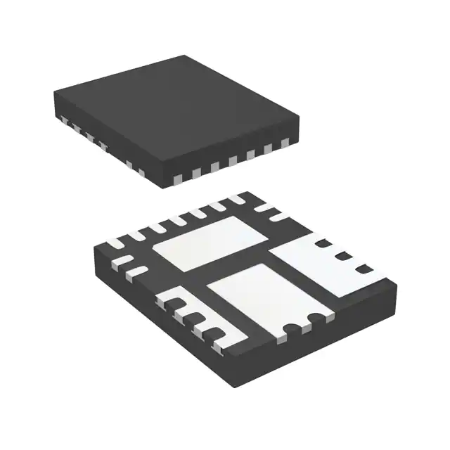
- Part No.:
- IR3870MTR1PBF
- Manufacturer:
- Infineon Technologies
- Package:
- 17-PowerVQFN
- Datasheet:
-
 IR3870MTR1PBF.pdf
- Description:
- IC REG BUCK ADJ 10A PQFN
- Quantity:
- Payment:

- Shipping:

Inventory:3,636
Please send an inquiry. Send us your inquiry, and we will respond immediately.
Product details
Overview
IR3870MTR1PBF from Infineon Technologies is a highly integrated synchronous buck regulator with integrated high- and low-side MOSFETs, constant on-time control, 10A continuous output current capability, 3V–26V input range, and 0.5V–12V programmable output voltage. It delivers precision regulation in notebook power delivery and battery-powered POL applications without external compensation.
For engineers reviewing the IR3870MTR1PBF datasheet, IR3870MTR1PBF pinout, IR3870MTR1PBF application, or IR3870MTR1PBF equivalent, key selection considerations include its gate-drive charge pump option for high-current efficiency, pre-bias startup support, ±1% 0.5V reference accuracy, and programmable switching frequency via feedforward resistor.
Technical Context
The IR3870MTR1PBF implements a constant on-time (COT) hysteretic control architecture with no external loop compensation required, enabling fast transient response and stable operation across wide load and input ranges. Its internal 14.7 mΩ upper and 6.2 mΩ lower MOSFETs (at PVCC = 5V, TJ = 25°C) reduce conduction loss and simplify layout.
Switching frequency is set by an external resistor (RFF) connected to the FF pin, supporting 100–1000 kHz operation. The device integrates a charge pump (CPO pin) to boost gate drive voltage, sustaining high efficiency at full 10A load while maintaining low quiescent current (1.2 mA VCC operating current) in active mode.
Key Specifications
| Parameter | Value and Actual Design Meaning |
|---|---|
| Input Voltage Range | 3V to 26V - supports wide-input industrial and battery-based systems including 12V/19V notebook rails. |
| Output Voltage Range | 0.5V to 12V - enables core voltage regulation for CPUs, GPUs, and SoCs with ±1% reference accuracy. |
| Continuous Output Current | 10A - delivered without airflow in 60°C ambient using integrated MOSFETs and thermal-enhanced QFN package. |
| Switching Frequency | 100–1000 kHz - programmable via RFF resistor; higher frequencies enable smaller output inductors and capacitors. |
| Reference Accuracy | ±1% at 0.5V - ensures tight output regulation critical for low-voltage digital loads. |
| On-Time Accuracy | 280–320 ns - tightly controlled timing enables consistent COT behavior across temperature and line variations. |
| Thermal Resistance θJA | 35°C/W - measured on standard 4-layer PCB, enabling reliable 10A operation with minimal heatsinking. |
Pinout & Package
IR3870MTR1PBF uses a thermally enhanced 5 mm × 6 mm, 23-pin Power QFN package with exposed thermal pad (PGND-connected) for efficient heat dissipation in space-constrained POL designs.
| Pin/Terminal | Circuit Role | Design Meaning |
|---|---|---|
| VIN | Main input supply rail | Accepts 3–26V DC; connects to bulk capacitor and feeds internal bias and gate drivers. |
| PHASE | Switching node | Connects to inductor; carries high dv/dt switching waveform; must be routed with minimal parasitic inductance. |
| BOOT | Bootstrap supply | Capacitor between BOOT and PHASE provides gate drive voltage for high-side MOSFET. |
| PVCC | Gate drive supply | 5V supply for internal gate drivers; decoupled with local ceramic capacitor. |
| VCC | Bias supply | 3.3V internal LDO output; powers control logic and reference circuitry. |
| FB | Feedback input | Resistor divider from VOUT sets regulated output; monitors over/under-voltage faults. |
| EN | Enable input | Active-high logic input with voltage monitoring; asserts shutdown if EN < 1.13V. |
| PGOOD | Power-good indicator | Open-drain output signaling valid regulation (VOUT within ±7.5% of target). |
| ISET | Current limit programming | Resistor to PHASE sets overcurrent trip threshold; enables precise OCP tuning. |
| SS | Soft-start control | Capacitor to GND sets output voltage ramp rate; prevents inrush current during startup. |
| GND / PGND | Signal / power ground | Separate pins minimize noise coupling; PGND connects to thermal pad and power return path. |
Key Features
| Feature | Design Value |
|---|---|
| No external compensation required | Constant on-time control eliminates need for feedback compensation network, reducing BOM count and layout sensitivity. |
| Pre-bias startup | Allows safe turn-on into pre-charged output capacitors without reverse current or voltage overshoot. |
| Charge pump gate drive option | Boosts high-side gate voltage above VIN, sustaining low RDS(on) and high efficiency at full 10A load. |
| Programmable fault protection | Adjustable overcurrent threshold (via ISET), plus fixed over/under-voltage lockout (±7.5% hysteresis on FB). |
| Ultra-low light-load efficiency | Maintains >85% efficiency at 0.1A output due to adaptive COT operation and low quiescent current (1.2 mA). |
Applications
| Notebook CPU Core Supply | Gaming Console SoC Rail |
|---|---|
Use Scenario: Regulating 0.8–1.2V core voltage for Intel/AMD mobile processors in thin-and-light notebooks. IC Role / Device Role / Timing Role: Primary point-of-load regulator delivering up to 10A with fast transient response and pre-bias startup. Use Value: Eliminates external compensation and reduces solution footprint by integrating dual MOSFETs and controller in 5×6mm QFN. | Use Scenario: Powering GPU and application processor cores in PlayStation/Xbox generation consoles with dynamic load steps. IC Role / Device Role / Timing Role: High-efficiency synchronous buck converter with programmable soft-start and PGOOD sequencing. Use Value: Charge pump option sustains >90% efficiency at 8–10A, minimizing thermal impact in sealed enclosures. |
| LCD TV Backlight Driver Bias | Industrial FPGA I/O Bank Supply |
Use Scenario: Generating stable 3.3V or 5V bias for LED driver ICs in smart TV mainboards. IC Role / Device Role / Timing Role: Secondary POL regulator with wide 3–26V input tolerance accommodating varying DC bus conditions. Use Value: ±1% reference and OVP/UVP protection ensure consistent backlight brightness and prevent panel damage. | Use Scenario: Providing configurable 1.2V/1.8V/2.5V supplies to Xilinx/Intel FPGA I/O banks in programmable logic controllers. IC Role / Device Role / Timing Role: Flexible, pin-strapped adjustable output regulator with robust fault reporting (PGOOD, OCP). Use Value: Programmable switching frequency allows EMI optimization in noise-sensitive factory automation environments. |
Equivalent & Alternatives
The following parts are listed as comparable options for similar synchronous buck regulator applications.
| Alternative Part | Technical Difference | Application Difference | Selection Advice |
|---|---|---|---|
| MP2451DT-LF-Z | 36V max input, 0.8A output, external MOSFETs required; no integrated power stage. | Suitable only for sub-1A loads; lacks charge pump, pre-bias startup, and 10A capability. | Select when cost sensitivity outweighs integration needs and output current < 1A. |
| TPS546B24RVFT | 16V max input, 40A output, PMBus interface, external compensation required. | Targeted at server VRMs; larger package (6×6mm), higher complexity, and no charge pump. | Choose for digitally managed, multi-phase high-current systems where telemetry and configurability are essential. |
Compared with MP2451DT-LF-Z and TPS546B24RVFT, the IR3870MTR1PBF uniquely balances 10A integration, ultra-low-light-load efficiency, and zero-compensation simplicity-making it optimal for compact, battery-aware, single-rail POL designs where thermal headroom and layout area are constrained.
Availability
IR3870MTR1PBF is available at Aetrix Electronics and suitable for notebook power delivery, gaming console SoC rails, and industrial FPGA I/O bank supplies requiring stable component supply, long-term lifecycle support, and RoHS-compliant packaging.
Supply support for IR3870MTR1PBF includes scheduled delivery planning, volume procurement assistance, BOM continuity management, traceable sourcing, and lifecycle availability coordination for OEM customers, industrial embedded developers, connected-device designers, and electronics production programs.
Manufacturer
Infineon Technologies is a German semiconductor leader specializing in power management, automotive MCUs, and RF solutions, with global manufacturing and quality certification to ISO/TS 16949 and IECQ QC 080000.
The SupIRBuck™ product line delivers fully integrated, high-current DC/DC regulators targeting space-constrained, high-efficiency point-of-load applications in computing, consumer, and industrial electronics.
FAQ
What is the maximum allowable junction temperature for continuous 10A operation?
The IR3870MTR1PBF has a maximum junction temperature rating of 150°C. At 10A continuous load with 12V input and 1.1V output, thermal testing shows junction temperatures remain below 115°C on a standard 4-layer PCB with 2 oz copper and 1 in² thermal pad area-well within safe margin under 60°C ambient with no forced airflow.
How does the charge pump (CPO) improve efficiency at high load?
The integrated charge pump boosts gate drive voltage for the high-side MOSFET beyond VIN, ensuring full enhancement even at low input voltages (e.g., 3V). This maintains low RDS(on) (~14.7 mΩ at 25°C), reducing conduction loss and sustaining >92% efficiency at 10A/1.1V output-unachievable with standard bootstrap-only drives.
Can the IR3870MTR1PBF start up into a pre-biased output?
Yes. The device supports true pre-bias startup: when enabled, it monitors the FB pin voltage and delays high-side switching until the output begins rising, preventing reverse current flow through the low-side MOSFET body diode and avoiding output voltage collapse or overshoot during hot-insertion scenarios.
Is the 0.5V reference internally trimmed, and what is its drift over temperature?
The 0.5V reference is laser-trimmed during wafer sort and specified at ±1% (0.495–0.505V) over –10°C to +125°C junction temperature. Typical drift across that range is < ±0.5%, verified by production test data and confirmed in Figure 5 of the datasheet showing <5mV output deviation from 1.1V setpoint over 0–10A load at multiple temperatures.
IR3870MTR1PBF Specifications
- Product attributes
- Attribute value
- Manufacturer:
- Infineon Technologies
- Series:
- SupIRBuck®
- Package/Case:
- 17-PowerVQFN
- Packaging:
- Tape & Reel (TR)
- Product Status:
- Obsolete
- Function:
- Step-Down
- Output Configuration:
- Positive
- Topology:
- Buck
- Output Type:
- Adjustable
- Number of Outputs:
- 1
- Voltage - Input (Min):
- 3V
- Voltage - Input (Max):
- 26V
- Voltage - Output (Min/Fixed):
- 0.5V
- Voltage - Output (Max):
- 12V
- Current - Output:
- 10A
- Frequency - Switching:
- Up to 1MHz
- Synchronous Rectifier:
- Yes
- Operating Temperature:
- -40°C ~ 150°C (TJ)
- Grade:
- -
- Qualification:
- -
- Mounting Type:
- Surface Mount
- Supplier Device Package:
- PQFN (5x6)
IR3870MTR1PBF FAQ
1.How can I place an order for IR3870MTR1PBF through Aetrix?
Please submit a Request for Quotation (RFQ) for IR3870MTR1PBF on Aetrix. Our sales agent will provide a competitive quotation and guide you through the order confirmation once you accept the terms.
2.Are the price and stock information for IR3870MTR1PBF reliable?
The price and inventory of IR3870MTR1PBF are updated periodically and may fluctuate due to market conditions. Stock and pricing data are typically refreshed every 24 hours. Quotation validity for IR3870MTR1PBF is usually 5 days.
3.What payment methods are accepted for IR3870MTR1PBF?
We accept Wire Transfer, PayPal, Credit Card, Western Union, MoneyGram, and Escrow for IR3870MTR1PBF transactions.
Note: Certain payment methods may incur a processing fee.
4.How is shipping managed for IR3870MTR1PBF?
IR3870MTR1PBF orders can be shipped via leading logistics carriers, including DHL, UPS, FedEx, TNT, or Registered Mail.
Once your IR3870MTR1PBF order is processed, you will receive an email with the shipment details and tracking number.
Note: Tracking information may take up to 24 hours to appear. Express delivery typically takes 3–5 business days.
5.How can I obtain technical support or documentation for IR3870MTR1PBF?
For technical support, including IR3870MTR1PBF datasheets, pinout diagrams, or application guidance, please contact our engineering support team. They can provide detailed documentation and assistance for your IR3870MTR1PBF requirements.
6.How does Aetrix verify that IR3870MTR1PBF is sourced from the original manufacturer or authorized distributors?
All IR3870MTR1PBF products on Aetrix are procured from qualified distributors and authorized channels. Our dedicated quality assurance team conducts strict verification, including traceability checks and, if necessary, third-party testing. This ensures that IR3870MTR1PBF meets industry standards.
7.What is the process for return or replacement of IR3870MTR1PBF?
All IR3870MTR1PBF units undergo pre-shipment inspection (PSI). If there is an issue with IR3870MTR1PBF, returns or replacements are accepted under the following conditions:
1.Quantity discrepancies, incorrect items, or visible external defects (such as breakage or corrosion), acknowledged by Aetrix.
2.The issue is reported within 90 days of delivery.
3.The IR3870MTR1PBF part is unused and in its original packaging.
Return procedure for IR3870MTR1PBF:
1.Submit a request within 90 days.
2.Obtain a Return Material Authorization (RMA) from Aetrix.
IR3870MTR1PBF Tags
-
TPS562201DDCR
Texas Instruments

-
MC34063ABD-TR
STMicroelectronics
-
TPS561201DDCR
Texas Instruments

-
MC33063ADR
Texas Instruments
-
MC34063ADR
Texas Instruments

-
TPS560200DBVR
Texas Instruments
-
AP3012KTR-G1
Diodes Incorporated
-
TLV61048DBVR
Texas Instruments
-
AZ34063UMTR-G1
Diodes Incorporated
-
TPS562200DDCR
Texas Instruments
-
AP62300TWU-7
Diodes Incorporated
-
MC34063EBD-TR
STMicroelectronics
Tech Hub

An engineering guide to LED driver operation, constant-current and constant-voltage outputs, linear and switching topologies, dimming, IC selection, calculations, replacement compatibility, and fault c…

Operational amplifier guide covering op amp basics, feedback, ideal vs real op amps, common configurations, buffer circuits, offset, bias current, gain-bandwidth, slew rate, rail-to-rail limits and sel…

Jumper cables guide covering safe connection order, red and black clamp placement, final ground connection, cable gauge, length, clamp quality, copper vs CCA cables, jump starter comparison and battery…

LDO regulator guide covering low dropout voltage, power dissipation, thermal design, PSRR, output noise, capacitor stability, adjustable LDO circuits, LDO vs buck converter and datasheet selection chec…

Conditional Access Module guide covering CAM meaning, CI/CI+ interface, smart card authorization, DVB security workflow, TV and set-top box compatibility, internal electronics, ESD protection, connecto…

Guide to electronic component obsolescence covering EOL risk, PCN/PDN notices, last-time buy planning, replacement options, form-fit-function validation, counterfeit risk and BOM lifecycle management.

18650 battery guide covering lithium-ion cell basics, 3.6V/3.7V voltage, 4.2V charging, mAh and Wh capacity, protected cells, chargers, BMS, series-parallel packs, holders, welding and sourcing checks.…

Hall effect sensor guide covering working principle, linear and digital sensors, Arduino circuits, current sensing, speed detection, automotive applications, A3144 examples, signal filtering and datash…

Product Change Notification guide for electronic components, covering PCN meaning, PCN vs PDN/EOL, common change types, risk levels, form-fit-function review, engineering validation, BOM control, LTB/L…

A practical guide to blend door actuators, covering HVAC function, symptoms, location, AC and heater issues, reset and calibration, replacement cost, electrical diagnosis, compatibility checks, and rep…


