
 My Inquiry
 My Account


Infineon Technologies IR3898MTR1PBF
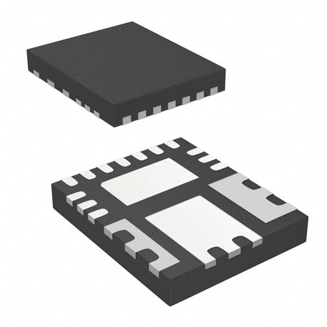
- Part No.:
- IR3898MTR1PBF
- Manufacturer:
- Infineon Technologies
- Package:
- 16-PowerVQFN
- Datasheet:
-
 IR3898MTR1PBF.pdf
- Description:
- IC REG BUCK ADJ 6A 16POWERQFN
- Quantity:
- Payment:

- Shipping:

Inventory:3,884
Please send an inquiry. Send us your inquiry, and we will respond immediately.
Product details
Overview
IR3898MTR1PBF from Infineon Technologies is a 6A synchronous buck regulator with integrated high- and low-side MOSFETs, programmable 300–1500 kHz switching frequency, 0.5 V ±0.5% reference accuracy, and operation across 1.0–21 V input range. It delivers regulated output from 0.5 V to 0.86×Vin in compact 4 mm × 5 mm PQFN, targeting point-of-load power in telecom servers and storage systems.
For engineers reviewing the IR3898MTR1PBF datasheet, IR3898MTR1PBF pinout, IR3898MTR1PBF application, or IR3898MTR1PBF equivalent, key selection criteria include thermally compensated current limit (70 mA short-circuit trip), monotonic start-up, pre-bias start capability, and Vp tracking/sourcing (±6 A) for multi-rail sequencing.
Technical Context
The IR3898 implements a voltage-mode PWM controller with feed-forward line regulation and an internal digital soft-start/soft-stop engine. Its error amplifier features 100–120 dB DC gain, 20–40 MHz GBWP, and ±1.5% input offset-enabling precise loop compensation via external R-C network on Comp/Fb pins.
Protection architecture includes zero-crossing comparator-based over-current detection (256/Fs delay), thermal shutdown, UVLO on Vcc (4.2 V turn-on) and Enable (1.2 V), and dual-threshold PGood with 1.28 ms turn-on delay and ±5% hysteresis relative to Vref or Vp.
Key Specifications
| Parameter | Value and Actual Design Meaning |
|---|---|
| Output Current | 6 A continuous; supports full-load efficiency optimization via smart LDO and thermally compensated hiccup-mode OCP. |
| Input Voltage Range | 1.0–21 V; wide range enables single-rail operation from 5 V or multi-rail bias via external Vcc. |
| Output Voltage Range | 0.5 V to 0.86×Vin; precision 0.5 V ±0.5% reference enables tight margining and tracking. |
| Switching Frequency | 300–1500 kHz; set by Rt resistor or synchronized externally; supports EMI control and inductor size reduction. |
| Package | 4 mm × 5 mm PQFN; 17-pin thermally enhanced layout with separate PGnd and signal Gnd pins. |
| Operating Temperature | −40 °C to +125 °C junction; qualified for industrial and telecom infrastructure environments. |
| Protection Features | Pre-bias start-up, OV/UV lockout, thermal shutdown, monotonic ramp, and robust hiccup-mode overcurrent (70 mA trip). |
Pinout & Package
IR3898MTR1PBF uses a 4 mm × 5 mm, 17-pin Power QFN (PQFN) package with exposed thermal pad. Pin 17 and Pin 4 are dedicated signal ground connections; Pin 11 is isolated power ground (PGnd) for MOSFET drivers; Pin 13 (PVin) and Pin 9 (Vin) support dual-input bias architecture.
| Pin/Terminal | Circuit Role | Design Meaning |
|---|---|---|
| Fb | Inverting input of error amplifier | Connects to output divider; sets Vout = 0.5 V × (1 + R1/R2); enables closed-loop regulation. |
| Vref | Internal 0.5 V reference output | Used for margining (0.4–1.2 V) or grounding in tracking mode; requires 100 pF bypass cap in normal use. |
| Comp | Error amplifier output | Drives external RC compensation network between Comp and Fb to stabilize control loop. |
| Rt/Sync | Frequency programming & sync input | Pull to Gnd via resistor (e.g., 39.2 kΩ → 600 kHz); accepts external clock via diode coupling. |
| S_Ctrl | Soft-start/soft-stop control | High = internal soft-start; low = controlled discharge; 2.4 V logic threshold ensures noise immunity. |
| PGood | Open-drain power-good status | Asserts after 1.28 ms when Vsns reaches 90% Vref; requires external 49.9 kΩ pull-up. |
| Vsns | Output voltage sense input | Optional alternative to Fb for PGood/OVP; connects directly to Vout or via divider for higher accuracy. |
| Vin | LDO input supply | Bias source for internal LDO; short to Vcc/LDO_Out if external 5–7.5 V supply is used. |
| Vcc/LDO_Out | Internal LDO output / external bias input | Provides 6.4 V typical bias; improves light/full-load efficiency; requires ≥2.2 µF ceramic capacitor. |
| PGnd | Power ground return | Isolated return path for high-current MOSFET drivers; must connect to system power ground plane. |
| SW | Switch node | Connects to output inductor; experiences fast dV/dt transitions; requires low-inductance layout. |
| Boot | High-side gate driver supply | Charged via internal bootstrap diode; requires 100 nF capacitor to SW for gate drive integrity. |
| Enable | Logic enable with UVLO | 1.2 V turn-on threshold; resistor divider from PVin enables input UVLO at system level. |
| Vp | Tracking reference input | Accepts external voltage for rail sequencing; ±6 A sourcing/sinking capability enables active tracking. |
| PVin | Main power stage input | Primary high-current input (1.0–21 V); maximum SW node voltage limited to 25 V DC. |
Key Features
| Feature | Design Value |
|---|---|
| Integrated MOSFET drivers + bootstrap diode | Eliminates external high-side gate drive components; reduces BOM count and layout complexity. |
| Smart internal LDO | Delivers 6.4 V bias with <0.7 V dropout; improves efficiency across 0–6 A load range vs. traditional bias schemes. |
| Thermally compensated current limit | Adjusts trip point with junction temperature; prevents false OCP during thermal transients while maintaining safety margin. |
| Enhanced pre-bias start-up | Allows safe startup into pre-charged output capacitors without reverse current or overshoot. |
| Programmable PGood with tracking | Configurable thresholds (85–125% Vref/Vp) and 1.28 ms delay ensure reliable system power sequencing. |
Applications
| Telecom Line Cards | Server Memory Modules |
|---|---|
Use Scenario: Powering FPGA I/O banks and SerDes interfaces on carrier-grade line cards requiring strict voltage tolerance and sequencing. IC Role / Device Role / Timing Role: Primary point-of-load regulator delivering 1.2 V @ 6 A with ±0.5% output accuracy and monotonic start-up. Use Value: Vp pin enables synchronized ramp with core voltage rails; PGood delay ensures clean power-up sequence before FPGA configuration. | Use Scenario: Supplying DDR4 memory termination voltage (VTT) and auxiliary rails on enterprise server DIMMs. IC Role / Device Role / Timing Role: Secondary buck converter providing 0.6 V VTT with pre-bias start and ±6 A Vp sink/source for dynamic load matching. Use Value: Thermally compensated OCP prevents false shutdown during burst memory access; smart LDO maintains efficiency at light loads. |
| Storage Controller Boards | Distributed PoL in Edge Routers |
Use Scenario: Regulating 3.3 V and 1.8 V supplies for SAS/SATA controller ASICs in enterprise SSD enclosures. IC Role / Device Role / Timing Role: Dual-output implementation using two IR3898s with synchronized switching (Rt/Sync) to minimize input ripple. Use Value: 600 kHz default frequency balances efficiency and EMI; external sync eliminates beat frequencies in multi-regulator systems. | Use Scenario: Local 1.0 V core supply for packet processing ASICs in compact edge routing hardware with space constraints. IC Role / Device Role / Timing Role: Compact 4 mm × 5 mm PQFN solution delivering 6 A in minimal PCB area; operates from 12 V intermediate bus. Use Value: Integrated bootstrap diode and drivers reduce component count by ≥4 vs. controller+driver+MOSFET discrete solution. |
Equivalent & Alternatives
The following parts are listed as comparable options for similar synchronous buck regulator applications.
| Alternative Part | Technical Difference | Application Difference | Selection Advice |
|---|---|---|---|
| MP2451DT-LF-Z (Monolithic Power) | 3 A rated, 2–24 V input, no integrated Vp tracking or smart LDO; smaller 3 mm × 3 mm QFN. | Lacks rail sequencing support and pre-bias start; suitable only for non-critical, lower-current PoL. | Select when cost and footprint are prioritized over sequencing, protection, and 6 A capability. |
| TPS546B24RVFT (Texas Instruments) | 6 A, 4–18 V input, PMBus interface, digital loop compensation; larger 5 mm × 5.5 mm VQFN. | Requires external EEPROM and firmware setup; adds telemetry but increases design complexity. | Select when digital monitoring, margining, and adaptive loop tuning are required over analog simplicity. |
Compared with MP2451DT-LF-Z and TPS546B24RVFT, the IR3898MTR1PBF offers analog simplicity with robust analog sequencing (Vp), pre-bias start, and thermally adaptive protection-ideal for high-reliability telecom and storage where deterministic analog behavior is preferred over digital overhead.
Availability
IR3898MTR1PBF is available at Aetrix Electronics and suitable for telecom line cards, server memory modules, and storage controller boards requiring stable component supply, long-lifecycle support, and RoHS-compliant packaging.
Supply support for IR3898MTR1PBF includes scheduled delivery planning, volume procurement assistance, BOM continuity management, traceable sourcing, and lifecycle availability coordination for OEM customers, industrial embedded developers, connected-device designers, and electronics production programs.
Manufacturer
Infineon Technologies is a German semiconductor manufacturer specializing in power management, automotive, and industrial control ICs, with global manufacturing and quality certification to ISO/TS 16949 and IECQ QC 080000.
The SupIRBuck™ product line delivers highly integrated DC/DC regulators targeting high-efficiency, space-constrained point-of-load applications in networking, computing, and data center infrastructure.
FAQ
What is the minimum output voltage supported by IR3898MTR1PBF?
The IR3898MTR1PBF supports a minimum output voltage of 0.5 V, set by its internal precision reference (0.5 V ±0.5%). This value is fixed and cannot be lowered further-even with external feedback resistors-because the error amplifier's reference is hardwired to 0.5 V. Output voltages below 0.5 V require a different regulator architecture.
Can IR3898MTR1PBF operate without an external bootstrap capacitor?
No. The IR3898MTR1PBF requires a 100 nF ceramic capacitor between Boot and SW pins to sustain high-side MOSFET gate drive. Omitting this capacitor causes immediate loss of high-side switching, resulting in no output voltage and potential device latch-up. The internal bootstrap diode charges this capacitor each cycle; no external diode is needed.
How does the Vp pin function during power sequencing?
The Vp pin serves as a tracking reference input with ±6 A sourcing/sinking capability. When an external voltage ramp (e.g., from another regulator) is applied to Vp, the IR3898 regulates its output to match that ramp-enabling precise voltage sequencing across multiple rails. In normal operation, Vp is left floating.
Is IR3898MTR1PBF compatible with ceramic output capacitors only?
Yes-the IR3898MTR1PBF is optimized for ceramic output capacitors (typical 22–100 µF total). Its control loop and ESR-independent compensation (via Comp/Fb network) eliminate reliance on capacitor ESR for stability. Aluminum or tantalum capacitors are not recommended due to higher ESR, which may degrade transient response and cause instability.
IR3898MTR1PBF Specifications
- Product attributes
- Attribute value
- Manufacturer:
- Infineon Technologies
- Series:
- SupIRBuck®
- Package/Case:
- 16-PowerVQFN
- Packaging:
- Tape & Reel (TR)
- Product Status:
- Obsolete
- Function:
- Step-Down
- Output Configuration:
- Positive
- Topology:
- Buck
- Output Type:
- Adjustable
- Number of Outputs:
- 1
- Voltage - Input (Min):
- 1V
- Voltage - Input (Max):
- 21V
- Voltage - Output (Min/Fixed):
- 0.5V
- Voltage - Output (Max):
- 18.06V
- Current - Output:
- 6A
- Frequency - Switching:
- 300kHz ~ 1.5MHz
- Synchronous Rectifier:
- Yes
- Operating Temperature:
- -40°C ~ 125°C (TJ)
- Grade:
- -
- Qualification:
- -
- Mounting Type:
- Surface Mount
- Supplier Device Package:
- 16-PowerQFN
IR3898MTR1PBF FAQ
1.How can I place an order for IR3898MTR1PBF through Aetrix?
Please submit a Request for Quotation (RFQ) for IR3898MTR1PBF on Aetrix. Our sales agent will provide a competitive quotation and guide you through the order confirmation once you accept the terms.
2.Are the price and stock information for IR3898MTR1PBF reliable?
The price and inventory of IR3898MTR1PBF are updated periodically and may fluctuate due to market conditions. Stock and pricing data are typically refreshed every 24 hours. Quotation validity for IR3898MTR1PBF is usually 5 days.
3.What payment methods are accepted for IR3898MTR1PBF?
We accept Wire Transfer, PayPal, Credit Card, Western Union, MoneyGram, and Escrow for IR3898MTR1PBF transactions.
Note: Certain payment methods may incur a processing fee.
4.How is shipping managed for IR3898MTR1PBF?
IR3898MTR1PBF orders can be shipped via leading logistics carriers, including DHL, UPS, FedEx, TNT, or Registered Mail.
Once your IR3898MTR1PBF order is processed, you will receive an email with the shipment details and tracking number.
Note: Tracking information may take up to 24 hours to appear. Express delivery typically takes 3–5 business days.
5.How can I obtain technical support or documentation for IR3898MTR1PBF?
For technical support, including IR3898MTR1PBF datasheets, pinout diagrams, or application guidance, please contact our engineering support team. They can provide detailed documentation and assistance for your IR3898MTR1PBF requirements.
6.How does Aetrix verify that IR3898MTR1PBF is sourced from the original manufacturer or authorized distributors?
All IR3898MTR1PBF products on Aetrix are procured from qualified distributors and authorized channels. Our dedicated quality assurance team conducts strict verification, including traceability checks and, if necessary, third-party testing. This ensures that IR3898MTR1PBF meets industry standards.
7.What is the process for return or replacement of IR3898MTR1PBF?
All IR3898MTR1PBF units undergo pre-shipment inspection (PSI). If there is an issue with IR3898MTR1PBF, returns or replacements are accepted under the following conditions:
1.Quantity discrepancies, incorrect items, or visible external defects (such as breakage or corrosion), acknowledged by Aetrix.
2.The issue is reported within 90 days of delivery.
3.The IR3898MTR1PBF part is unused and in its original packaging.
Return procedure for IR3898MTR1PBF:
1.Submit a request within 90 days.
2.Obtain a Return Material Authorization (RMA) from Aetrix.
IR3898MTR1PBF Tags
-
TPS562201DDCR
Texas Instruments

-
MC34063ABD-TR
STMicroelectronics
-
TPS561201DDCR
Texas Instruments

-
MC33063ADR
Texas Instruments
-
MC34063ADR
Texas Instruments

-
TPS560200DBVR
Texas Instruments
-
AP3012KTR-G1
Diodes Incorporated
-
TLV61048DBVR
Texas Instruments
-
AZ34063UMTR-G1
Diodes Incorporated
-
TPS562200DDCR
Texas Instruments
-
AP62300TWU-7
Diodes Incorporated
-
MC34063EBD-TR
STMicroelectronics
Tech Hub

Operational amplifier guide covering op amp basics, feedback, ideal vs real op amps, common configurations, buffer circuits, offset, bias current, gain-bandwidth, slew rate, rail-to-rail limits and sel…

Jumper cables guide covering safe connection order, red and black clamp placement, final ground connection, cable gauge, length, clamp quality, copper vs CCA cables, jump starter comparison and battery…

LDO regulator guide covering low dropout voltage, power dissipation, thermal design, PSRR, output noise, capacitor stability, adjustable LDO circuits, LDO vs buck converter and datasheet selection chec…

Conditional Access Module guide covering CAM meaning, CI/CI+ interface, smart card authorization, DVB security workflow, TV and set-top box compatibility, internal electronics, ESD protection, connecto…

Guide to electronic component obsolescence covering EOL risk, PCN/PDN notices, last-time buy planning, replacement options, form-fit-function validation, counterfeit risk and BOM lifecycle management.

18650 battery guide covering lithium-ion cell basics, 3.6V/3.7V voltage, 4.2V charging, mAh and Wh capacity, protected cells, chargers, BMS, series-parallel packs, holders, welding and sourcing checks.…

Hall effect sensor guide covering working principle, linear and digital sensors, Arduino circuits, current sensing, speed detection, automotive applications, A3144 examples, signal filtering and datash…

Product Change Notification guide for electronic components, covering PCN meaning, PCN vs PDN/EOL, common change types, risk levels, form-fit-function review, engineering validation, BOM control, LTB/L…

A practical guide to blend door actuators, covering HVAC function, symptoms, location, AC and heater issues, reset and calibration, replacement cost, electrical diagnosis, compatibility checks, and rep…

Engineering guide to Raspberry Pi alternatives, covering chip-level differences, Orange Pi, ROCK, Jetson, Banana Pi, NanoPi, Compute Module, Pico, GPIO, camera, HAT compatibility, and replacement risks…


