
 My Inquiry
 My Account


Renesas ISL23325TFRUZ-TK
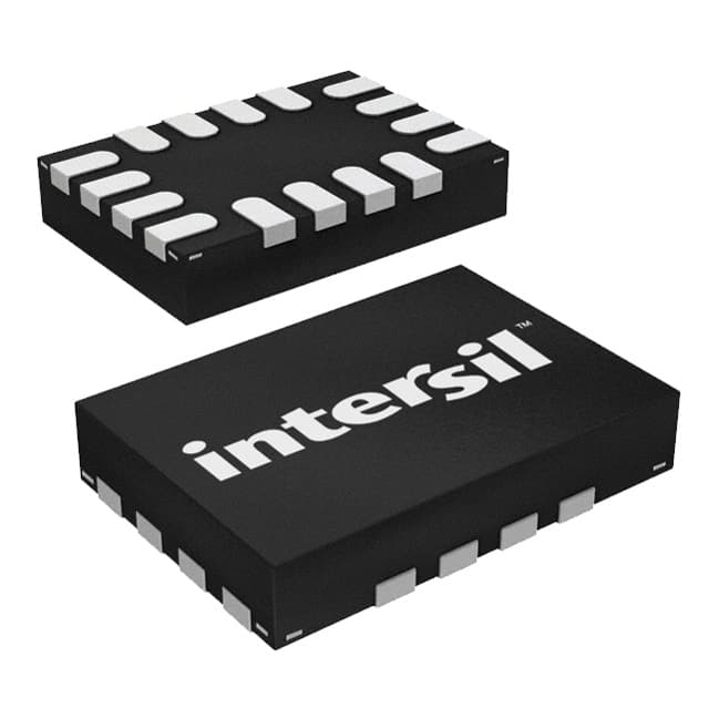
- Part No.:
- ISL23325TFRUZ-TK
- Manufacturer:
- Renesas
- Category:
- Digital Potentiometers
- Package:
- 16-UFQFN
- Datasheet:
-
 ISL23325TFRUZ-TK.pdf
- Description:
- IC DGTL POT 100KOHM 16UTQFN
- Quantity:
- Payment:

- Shipping:

Inventory:4,514
Please send an inquiry. Send us your inquiry, and we will respond immediately.
Product details
Overview
ISL23325TFRUZ-TK from Renesas (formerly Intersil) is a dual, volatile, 256-tap digitally controlled potentiometer with I²C interface, 100kΩ end-to-end resistance, 16-pin µTQFN package, and extended industrial temperature range (–40°C to +125°C). It operates from 1.7V to 5.5V analog supply (VCC) and 1.2V to 5.5V logic supply (VLOGIC), enabling direct low-voltage bus interfacing without level shifters - ideal for precision trimming in battery-powered instrumentation and power supply margining.
For engineers reviewing the ISL23325TFRUZ-TK datasheet, ISL23325TFRUZ-TK pinout, ISL23325TFRUZ-TK application, or ISL23325TFRUZ-TK equivalent, key selection considerations include its dual-channel architecture, wiper register volatility, shutdown mode behavior, 70Ω typical wiper resistance at 3.3V, and guaranteed monotonicity in both voltage divider and rheostat modes.
Technical Context
The ISL23325TFRUZ-TK integrates two independent DCP cores on a monolithic CMOS die, each with an 8-bit volatile Wiper Register (WR0/WR1) directly accessible via I²C. Wiper positioning uses make-before-break switching, ensuring glitch-free transitions during tap changes. Power-on defaults WR0 and WR1 to 0x80 (mid-scale, 128), guaranteeing known initial output impedance.
Its dual-supply architecture separates analog (VCC) and digital (VLOGIC) domains: VLOGIC enables 1.2V I²C compatibility while VCC supports up to 5.5V DCP terminal voltage. Shutdown mode disconnects RH/RL paths and internally connects RW to RL via a 2kΩ resistor, reducing leakage and isolating the wiper from external circuitry.
Key Specifications
| Parameter | Value and Actual Design Meaning |
|---|---|
| Total Resistance | 100kΩ ±20% - defines full-scale adjustment range for gain/offset tuning circuits |
| Wiper Resistance | 70Ω typical @ VCC = 3.3V - limits insertion error and signal attenuation in precision voltage dividers |
| Integral Non-linearity | ±0.15 LSB (U/T options) - ensures <0.06% linearity error across 256 taps for calibration-critical applications |
| VCC Supply Range | 1.7V to 5.5V - supports single-cell Li-ion, 3.3V, and 5V systems without external regulators |
| VLOGIC Supply Range | 1.2V to 5.5V - allows direct connection to 1.2V/1.8V/3.3V microcontrollers without level translation |
| Standby Current | 1.2µA @ VCC = 1.7V, VLOGIC = 1.2V - enables ultra-low-power operation in always-on sensor nodes |
| Temperature Range | –40°C to +125°C - qualified for under-hood automotive, industrial motor control, and telecom infrastructure |
Pinout & Package
ISL23325TFRUZ-TK is housed in a RoHS-compliant 16-lead µTQFN (2.6mm × 1.8mm, 0.5mm pitch) package with wettable flanks. Pin 7 is NC (not connected); all other pins are electrically functional as defined below.
| Pin/Terminal | Circuit Role | Design Meaning |
|---|---|---|
| GND (Pin 1) | Ground reference | Common return path for analog and digital sections; must be low-impedance to minimize noise coupling |
| VLOGIC (Pin 2) | Digital supply input | Powers I²C interface and internal level shifter; sets logic threshold for SDA/SCL/A0–A2 |
| RH1 (Pin 3) | DCP1 high terminal | Fixed end of Potentiometer 1; connects to higher potential in voltage divider or bias network |
| GND (Pin 4) | Ground reference | Second ground pin for improved thermal and electrical performance in compact layouts |
| NC (Pin 5) | No connect | Internally unconnected; must remain floating or tied to GND per layout best practices |
| RL1 (Pin 6) | DCP1 low terminal | Fixed end of Potentiometer 1; connects to lower potential or system ground |
| RW1 (Pin 7) | DCP1 wiper output | Movable terminal of Potentiometer 1; delivers adjustable voltage/resistance based on WR1 value |
| VCC (Pin 8) | Analog supply input | Powers resistor array and CMOS switches; sets maximum allowable voltage across RH/RL/RW |
| A1 (Pin 9) | I²C address bit | Hardwired slave address bit (A1); combines with A0/A2 to select one of eight devices on shared bus |
| RW0 (Pin 10) | DCP0 wiper output | Movable terminal of Potentiometer 0; independently controllable via WR0 register |
| SCL (Pin 11) | I²C clock input | Open-drain input requiring external pull-up; synchronizes data transfer at up to 400kHz |
| RH0 (Pin 12) | DCP0 high terminal | Fixed end of Potentiometer 0; used for dual-gain or dual-bias configurations |
| RL0 (Pin 13) | DCP0 low terminal | Fixed end of Potentiometer 0; completes first potentiometer leg |
| SDA (Pin 14) | I²C bidirectional data | Open-drain input/output requiring external pull-up; carries address, command, and register data |
| A0 (Pin 15) | I²C address bit | Hardwired slave address bit (A0); determines unique I²C address when multiple units share bus |
| A2 (Pin 16) | I²C address bit | Hardwired slave address bit (A2); enables up to eight ISL23325 devices on same I²C bus |
Key Features
| Feature | Design Value |
|---|---|
| Dual 256-tap DCPs | Enables simultaneous independent adjustment of two analog parameters (e.g., gain + offset) in single IC |
| Volatile wiper registers | WR0/WR1 reset to 0x80 on power-up - guarantees repeatable mid-scale startup without external initialization |
| Independent VCC/VLOGIC supplies | Eliminates need for level shifters when interfacing 1.2V/1.8V MCUs with 3.3V/5V analog rails |
| Shutdown mode | Forces open-circuit RH–RL path and connects RW to RL via 2kΩ - prevents unintended loading during sleep |
| Monotonicity guarantee | Ensures DNL ≤ ±0.4 LSB across full temperature range - critical for closed-loop feedback stability |
| Low wiper resistance | 70Ω typical at 3.3V minimizes voltage drop and nonlinearity in high-precision voltage divider topologies |
Applications
| Power Supply Margining | Sensor Circuit Trimming |
|---|---|
|
Use Scenario: Adjusting reference voltage thresholds in DC-DC converter feedback loops to validate tolerance margins under load transients. IC Role / Device Role / Timing Role: Dual DCP provides independent fine-tuning of upper/lower trip points in overvoltage/undervoltage protection circuits. Use Value: Enables automated margin testing without manual resistor changes; 100kΩ resistance supports high-impedance feedback networks minimizing current draw. |
Use Scenario: Calibrating offset and gain errors in bridge-based pressure or temperature sensors before ADC digitization. IC Role / Device Role / Timing Role: ISL23325TFRUZ-TK acts as programmable offset null and span adjust in analog front-end signal conditioning. Use Value: 0.06% INL and monotonic response ensure calibration accuracy remains stable across –40°C to +125°C operating range. |
| Battery-Powered Instrument Gain | RF Power Amplifier Bias |
|
Use Scenario: Dynamically scaling amplifier gain in portable multimeters or handheld oscilloscopes to maintain optimal ADC input range. IC Role / Device Role / Timing Role: Configurable rheostat mode (RW–RL) sets transimpedance gain in photodiode amplifiers or programmable gain stages. Use Value: 1.2µA standby current extends battery life; 1.2V–5.5V VLOGIC allows direct interface with ultra-low-power microcontrollers. |
Use Scenario: Compensating for temperature-induced drift in GaAs FET bias networks to stabilize RF output power. IC Role / Device Role / Timing Role: Voltage divider mode (RH–RL–RW) adjusts gate bias voltage in Class AB RF PAs to maintain constant quiescent current. Use Value: 45ppm/°C end-to-end tempco (T option) and 2.3ppm/°C ratiometric tempco minimize drift-induced gain compression. |
Equivalent & Alternatives
The following parts are listed as comparable options for similar digitally controlled potentiometer applications.
| Alternative Part | Technical Difference | Application Difference | Selection Advice |
|---|---|---|---|
| AD5242BRUZ100 | Non-volatile EEPROM storage; 100kΩ; 24-lead TSSOP; no VLOGIC pin - requires external level shifting for sub-1.8V buses | Preferred where power-loss retention is required; unsuitable for 1.2V I²C systems without translation | Select AD5242BRUZ100 only if non-volatility and EEPROM endurance (>100k cycles) outweigh need for 1.2V bus compatibility |
| MCP45HV51-103E/MS | High-voltage rating (up to 36V); 10kΩ; 8-bit resolution; 8-lead MSOP; no shutdown mode; VDD-only supply | Targeted at industrial PLC analog I/O modules needing >12V rail support; lacks low-voltage flexibility | Choose MCP45HV51-103E/MS only when DCP terminals must withstand >12V; not suitable for battery-powered 1.2V–3.3V designs |
Compared with AD5242BRUZ100 and MCP45HV51-103E/MS, the ISL23325TFRUZ-TK uniquely supports 1.2V I²C operation without level shifters, offers dual-channel integration in a 2.6×1.8mm footprint, and provides hardware shutdown isolation - making it optimal for space-constrained, ultra-low-power, multi-rail embedded systems.
Availability
ISL23325TFRUZ-TK is available at Aetrix Electronics and suitable for power supply margining, sensor trimming, battery-powered instrument gain adjustment, and RF amplifier bias compensation requiring stable component supply across extended temperature ranges and low-voltage I²C ecosystems.
Supply support for ISL23325TFRUZ-TK includes scheduled delivery planning, volume procurement assistance, BOM continuity management, traceable sourcing, and lifecycle availability coordination for OEM customers, industrial embedded developers, connected-device designers, and electronics production programs.
Manufacturer
Renesas Electronics Corporation acquired Intersil in 2017 and maintains legacy product lines including precision analog ICs. Renesas is a global semiconductor leader focused on embedded processing, analog, power, and connectivity solutions.
The ISL23325TFRUZ-TK belongs to Renesas' XDCP™ (eXternally Digitally Controlled Potentiometer) family, designed specifically for replacing mechanical potentiometers in automated calibration, adaptive biasing, and programmable analog signal conditioning applications.
FAQ
What is the default wiper position of ISL23325TFRUZ-TK after power-on?
Upon power-up, both wiper registers (WR0 and WR1) of the ISL23325TFRUZ-TK reset to 0x80 (decimal 128), placing each wiper at the exact mid-scale position between RH and RL terminals. This behavior is guaranteed by internal power-on reset circuitry and ensures repeatable startup conditions without host MCU intervention.
Does ISL23325TFRUZ-TK support true 1.2V I²C communication?
Yes - the ISL23325TFRUZ-TK's dedicated VLOGIC pin accepts 1.2V to 5.5V, enabling direct connection to 1.2V I²C masters without external level shifters. Its input thresholds scale with VLOGIC (VIH = 0.7×VLOGIC), and SDA/SCL operate reliably at 400kHz even at 1.2V, as verified in the FN7870 datasheet.
Can ISL23325TFRUZ-TK be used in rheostat mode?
Yes - the ISL23325TFRUZ-TK supports rheostat configuration by connecting either RH or RL to the same node and using RW and the remaining terminal. In this mode, it delivers monotonic resistance adjustment from near-zero to 100kΩ with RINL ≤ ±1.0 MI and RDNL ≤ ±0.5 MI across the full temperature range.
What happens to the wiper state during ISL23325TFRUZ-TK shutdown mode?
In shutdown mode (SHDN bit = 0 in ACR), the ISL23325TFRUZ-TK disconnects the RH–RL resistor string and internally connects RW to RL through a 2kΩ series resistor. Critically, the WR0 and WR1 register values are retained, so wipers return to their pre-shutdown positions upon exit - preserving calibration state.
Is ISL23325TFRUZ-TK compatible with standard I²C bus addressing?
Yes - the ISL23325TFRUZ-TK implements a standard 7-bit I²C slave address with three hardware-configurable bits (A2, A1, A0), allowing up to eight devices on a single bus. Its address format follows I²C specification, and it responds to general call and write/read operations per the FN7870 protocol timing diagrams.
ISL23325TFRUZ-TK Specifications
- Product attributes
- Attribute value
- Manufacturer:
- Renesas
- Series:
- XDCP™
- Package/Case:
- 16-UFQFN
- Packaging:
- Tape & Reel (TR)
- Product Status:
- Active
- Programmable:
- Not Verified
- Taper:
- Linear
- Configuration:
- Potentiometer
- Number of Circuits:
- 2
- Number of Taps:
- 256
- Resistance (Ohms):
- 100k
- Interface:
- I2C
- Memory Type:
- Volatile
- Voltage - Supply:
- 1.2V ~ 5.5V, 1.7V ~ 5.5V
- Features:
- Selectable Address
- Tolerance:
- ±20%
- Temperature Coefficient (Typ):
- 45ppm/°C
- Mounting Type:
- Surface Mount
- Grade:
- -
- Qualification:
- -
- Supplier Device Package:
- 16-UTQFN (2.6x1.8)
- Operating Temperature:
- -40°C ~ 125°C
- Resistance - Wiper (Ohms) (Typ):
- 70
ISL23325TFRUZ-TK FAQ
1.How can I place an order for ISL23325TFRUZ-TK through Aetrix?
Please submit a Request for Quotation (RFQ) for ISL23325TFRUZ-TK on Aetrix. Our sales agent will provide a competitive quotation and guide you through the order confirmation once you accept the terms.
2.Are the price and stock information for ISL23325TFRUZ-TK reliable?
The price and inventory of ISL23325TFRUZ-TK are updated periodically and may fluctuate due to market conditions. Stock and pricing data are typically refreshed every 24 hours. Quotation validity for ISL23325TFRUZ-TK is usually 5 days.
3.What payment methods are accepted for ISL23325TFRUZ-TK?
We accept Wire Transfer, PayPal, Credit Card, Western Union, MoneyGram, and Escrow for ISL23325TFRUZ-TK transactions.
Note: Certain payment methods may incur a processing fee.
4.How is shipping managed for ISL23325TFRUZ-TK?
ISL23325TFRUZ-TK orders can be shipped via leading logistics carriers, including DHL, UPS, FedEx, TNT, or Registered Mail.
Once your ISL23325TFRUZ-TK order is processed, you will receive an email with the shipment details and tracking number.
Note: Tracking information may take up to 24 hours to appear. Express delivery typically takes 3–5 business days.
5.How can I obtain technical support or documentation for ISL23325TFRUZ-TK?
For technical support, including ISL23325TFRUZ-TK datasheets, pinout diagrams, or application guidance, please contact our engineering support team. They can provide detailed documentation and assistance for your ISL23325TFRUZ-TK requirements.
6.How does Aetrix verify that ISL23325TFRUZ-TK is sourced from the original manufacturer or authorized distributors?
All ISL23325TFRUZ-TK products on Aetrix are procured from qualified distributors and authorized channels. Our dedicated quality assurance team conducts strict verification, including traceability checks and, if necessary, third-party testing. This ensures that ISL23325TFRUZ-TK meets industry standards.
7.What is the process for return or replacement of ISL23325TFRUZ-TK?
All ISL23325TFRUZ-TK units undergo pre-shipment inspection (PSI). If there is an issue with ISL23325TFRUZ-TK, returns or replacements are accepted under the following conditions:
1.Quantity discrepancies, incorrect items, or visible external defects (such as breakage or corrosion), acknowledged by Aetrix.
2.The issue is reported within 90 days of delivery.
3.The ISL23325TFRUZ-TK part is unused and in its original packaging.
Return procedure for ISL23325TFRUZ-TK:
1.Submit a request within 90 days.
2.Obtain a Return Material Authorization (RMA) from Aetrix.
ISL23325TFRUZ-TK Tags
-
MCP4018T-103E/LT
Microchip Technology
-
MCP4018T-503E/LT
Microchip Technology

-
MCP4011T-103E/SN
Microchip Technology
-
MCP4018T-104E/LT
Microchip Technology
-
MCP4017T-503E/LT
Microchip Technology
-
MCP4018T-502E/LT
Microchip Technology
-
MCP4017T-103E/LT
Microchip Technology

-
MCP4531T-103E/MF
Microchip Technology
-
MCP4021T-202E/SN
Microchip Technology

-
MCP4023T-103E/CH
Microchip Technology
-
MCP4022T-503E/CH
Microchip Technology

-
MCP4551T-502E/MS
Microchip Technology
Tech Hub

TTL and CMOS logic families differ in thresholds, loading, output drive, power and timing. This engineering guide compares 74HC and 74HCT, calculates noise margins and checks 3.3 V/5 V compatibility.

A practical engineering guide to 3.3V and 5V logic compatibility, input thresholds, resistor dividers, translator ICs, MOSFET level shifting, I2C pull-ups, timing limits and power-sequencing risks.

The 74HC595 uses push-pull logic outputs, while the TPIC6B595 uses 50 V open-drain DMOS sinks for higher-power loads. This guide compares timing, current limits, 3.3 V interfacing, load wiring, thermal…

The 74HC595 converts serial data into eight stable parallel outputs. This guide covers pin functions, shift and storage timing, OE and MR behavior, drive-current limits, cascading, voltage compatibilit…

A technical comparison of level-sensitive latches and edge-triggered flip-flops, covering timing windows, setup and hold limits, master–slave operation, time borrowing, race-through, HDL inference and…

A D latch stores one bit while Enable controls when data can pass. This reference covers gate-level operation, truth tables, transparency, setup and hold timing, LE versus OE, common ICs and practical …

An SR latch stores one bit through cross-coupled feedback. This engineering reference covers NOR and NAND implementations, truth tables, forbidden-state recovery, gated operation, switch debouncing, fa…

Latch circuits retain one bit through feedback. This technical reference covers SR and D latches, truth tables, transparency, timing limits, latch-versus-flip-flop behavior, applications and common log…

An engineering guide to LED driver operation, constant-current and constant-voltage outputs, linear and switching topologies, dimming, IC selection, calculations, replacement compatibility, and fault c…

Operational amplifier guide covering op amp basics, feedback, ideal vs real op amps, common configurations, buffer circuits, offset, bias current, gain-bandwidth, slew rate, rail-to-rail limits and sel…


