
 My Inquiry
 My Account


Renesas ISL36111DRZ-T7
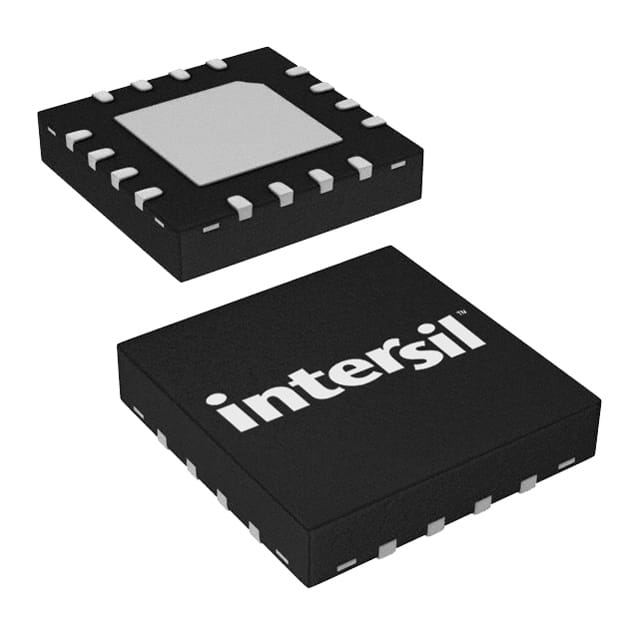
- Part No.:
- ISL36111DRZ-T7
- Manufacturer:
- Renesas
- Category:
- Specialized
- Package:
- 16-VFQFN Exposed Pad
- Datasheet:
-
 ISL36111DRZ-T7.pdf
- Description:
- IC INTERFACE SPECIALIZED 16QFN
- Quantity:
- Payment:

- Shipping:

Inventory:4,591
Please send an inquiry. Send us your inquiry, and we will respond immediately.
Product details
Overview
ISL36111DRZ-T7 from Renesas Electronics (formerly Intersil) is a single-channel 11.1 Gb/s receive-side lane extender IC designed for high-speed serial interconnects in active copper cable assemblies. It features CML I/O, adjustable equalization boost via two control pins, 1.2V supply operation, and integrated Loss-of-Signal (LOSB) detection. It extends signal reach up to 10m on 28AWG twin-axial cable in SFP+/QSFP modules.
For engineers reviewing the ISL36111DRZ-T7 datasheet, ISL36111DRZ-T7 pinout, ISL36111DRZ-T7 application, or ISL36111DRZ-T7 equivalent, key selection criteria include its fixed 3mm×3mm 16-lead QFN package, support for NRZ data rates from 1 to 11.1 Gb/s, low latency (<500 ps), 110 mW typical power consumption, and line-silence preservation capability for protocol-compliant idle states.
Technical Context
The ISL36111DRZ-T7 implements a settable analog equalizer followed by a limiting amplifier to compensate for frequency-dependent channel loss-including skin and dielectric effects-without adaptive convergence delay. Its equalization boost level is statically configured via CP[A,B] pins, enabling deterministic first-bit response across 9 discrete settings.
It uses CML input/output buffers with 100 Ω differential input resistance and 105 Ω typical differential output impedance, supports DC-coupled operation with internal VDD biasing of inputs, and integrates a voltage-controlled signal detector that drives both LOSB assertion and output muting based on the DT pin reference threshold.
Key Specifications
| Parameter | Value and Actual Design Meaning |
|---|---|
| Data Rate | 1 to 11.1 Gb/s NRZ - supports full range from 1G Ethernet to 10G/11.1G protocols including 10GBASE-CR, Fibre Channel, and 64b/66b encoded links. |
| Supply Voltage | 1.2 V ±0.1 V - single-rail operation enables direct integration into low-voltage 1.2V system domains without level-shifting. |
| Power Consumption | ~110 mW typical - enables thermal feasibility in high-density active cable modules with minimal heatsinking. |
| Propagation Delay | <500 ps - preserves timing budgets in ultra-low-latency interconnects such as HPC and switch fabric applications. |
| Input Amplitude Range | 600–1600 mVP-P differential - accommodates degraded signals after up to ~27 dB loss at 5 GHz (e.g., 10m 28AWG cable). |
| Output Residual Jitter | 0.35 UI at 10.3125 Gb/s - ensures sufficient jitter margin for downstream CDR lock in compliant receivers. |
| Operating Temperature | 0°C to +85°C ambient - validated for commercial-grade active cable module deployment in datacenter environments. |
Pinout & Package
ISL36111DRZ-T7 is housed in a 3 mm × 3 mm, 16-lead QFN package (L16.3x3B) with exposed thermal pad. The package is RoHS-compliant, Pb-free, and rated MSL3 per JEDEC J-STD-020.
| Pin/Terminal | Circuit Role | Design Meaning |
|---|---|---|
| VDD (Pins 1, 9, 12) | Power supply input | Three dedicated 1.2V supply pins requiring local 47nF + 100pF parallel decoupling for broadband noise suppression. |
| IN[P], IN[N] (Pins 2, 3) | Differential CML input | DC-biased to VDD; accepts 600–1600 mVP-P NRZ signals; requires 100nF AC-coupling capacitors with ≥6 GHz response. |
| LOSB (Pin 4) | Active-low LOS indicator | Open-drain output pulled HIGH internally (11 kΩ); asserts LOW when input falls below DT-set threshold. |
| CPA, CPB (Pins 6, 7) | Equalizer boost control | 2-bit static configuration inputs (MSB/LSB); float/GND/VDD combinations select one of nine boost levels (0–8). |
| GND (Pins 5, 8, 13, 16) | Ground reference | Four dedicated ground terminals; must be connected directly to low-impedance PCB ground plane for signal integrity. |
| OUT[P], OUT[N] (Pins 10, 11) | Differential CML output | Provides 450–850 mVP-P swing into 50 Ω loads; requires 100nF AC-coupling and matched 100 Ω differential routing. |
| DT (Pin 15) | Detection threshold reference | Analog input setting LOS sensitivity; tied to external resistor (e.g., 30 kΩ for >12 dB loss channels) to define mute threshold. |
Key Features
| Feature | Design Value |
|---|---|
| Adjustable equalization boost | 9 discrete, pin-configurable gain settings eliminate need for firmware or adaptation logic-ensures deterministic startup and immunity to pathological patterns. |
| Line silence preservation | Hardware-based muting during electrical idle maintains DC balance and protocol compliance (e.g., IEEE 802.3ae) without distorting quiescent states. |
| Integrated LOS detection | Single-pin LOSB output provides standardized loss-of-signal signaling for host controller monitoring in SFP+/QSFP modules. |
| Low-latency signal path | <500 ps propagation delay enables use in timing-critical backplane and chip-to-chip links where jitter accumulation must be minimized. |
| Compact 3mm×3mm QFN | Enables straight-through routing in ultra-thin active cable assemblies; reduces PCB real estate and improves density in multi-lane modules. |
Applications
| SFP+ Active Copper Cable Modules | QSFP Active Copper Cable Modules |
|---|---|
|
Use Scenario: Extending 10GBASE-CR reach beyond passive cable limits in top-of-rack switch interconnects. IC Role / Device Role / Timing Role: Receive-side lane extender restoring signal integrity after channel loss on 28AWG twin-axial cable. Use Value: Enables 10m reach at 10.3125 Gb/s with BER <10−12, eliminating need for thicker, heavier cables while maintaining SFP+ MSA compliance. |
Use Scenario: Signal conditioning in 40G QSFP active cables used for spine-leaf fabric interconnects. IC Role / Device Role / Timing Role: Single-channel equalizer per lane supporting 10.3125 Gb/s per lane in 4-lane architecture. Use Value: Delivers consistent 0.35 UI residual jitter across all lanes, ensuring reliable CDR lock and link training in multi-lane systems. |
| 10G Ethernet Backplane Traces | Fibre Channel Interconnects |
|
Use Scenario: Compensating for FR4 trace loss in midplane or motherboard traces between switch ASIC and front-panel cage. IC Role / Device Role / Timing Role: On-board equalizer placed adjacent to receiver to restore high-frequency content attenuated over 20+ cm PCB runs. Use Value: Supports 10GBASE-KR compliance with <12 dB insertion loss at 5 GHz, reducing layer count and cost vs. alternative equalization schemes. |
Use Scenario: Signal restoration in 8G/16G Fibre Channel active cables connecting storage arrays to directors. IC Role / Device Role / Timing Role: Protocol-transparent lane extender preserving FC-PI-4 encoding and idle sequences. Use Value: Maintains line-silence integrity during FC link initialization and idle periods, preventing spurious link resets or retraining events. |
Equivalent & Alternatives
The following parts are listed as comparable options for similar lane extender applications.
| Alternative Part | Technical Difference | Application Difference | Selection Advice |
|---|---|---|---|
| MAX3785ETE+ | Fixed-gain 10.3 Gb/s equalizer; no external boost control; higher 150 mW power; 16-pin TQFN but different pinout. | Lacks line-silence preservation and DT-adjustable LOS; suited for simpler point-to-point links without protocol idle requirements. | Select MAX3785ETE+ only if static equalization suffices and LOSB functionality is not required. |
| TI DS100BR410 | Quad-channel 10.3 Gb/s repeater with auto-adaptive equalization; 3.3V supply; 40-pin QFN; includes retiming and output de-emphasis. | Supports retiming and multi-lane synchronization; not pin-compatible; requires additional power rails and configuration interface. | Choose DS100BR410 when retiming or multi-lane coordination is needed-ISL36111DRZ-T7 remains optimal for low-latency, low-power, single-channel extension. |
Compared with MAX3785ETE+ and DS100BR410, the ISL36111DRZ-T7 uniquely balances ultra-low latency (<500 ps), static configurability, line-silence preservation, and 1.2V operation-making it the preferred choice for space-constrained, protocol-sensitive active copper cable designs where deterministic behavior and minimal power are critical.
Availability
ISL36111DRZ-T7 is available at Aetrix Electronics and suitable for SFP+ active cable modules, QSFP interconnects, and 10G Ethernet backplane trace extension requiring stable component supply, long-term lifecycle assurance, and RoHS-compliant packaging.
Supply support for ISL36111DRZ-T7 includes scheduled delivery planning, volume procurement assistance, BOM continuity management, traceable sourcing, and lifecycle availability coordination for OEM customers, industrial embedded developers, connected-device designers, and electronics production programs.
Manufacturer
Renesas Electronics Corporation is a global leader in microcontrollers, analog, power, and connectivity solutions, serving automotive, industrial, infrastructure, and datacenter markets with high-reliability semiconductor products.
The ISL36111DRZ-T7 belongs to Renesas' Q:ACTIVE lane extender product line, engineered specifically to transform passive copper cabling into intelligent, reach-extended interconnects for next-generation datacenters-emphasizing low power, low latency, and protocol-aware signal integrity.
FAQ
What data rates does the ISL36111DRZ-T7 support?
The ISL36111DRZ-T7 supports NRZ data rates from 1 Gb/s up to 11.1 Gb/s, including 1, 2.5, 3.125, 4.25, 5, 6.25, 8.5, 10.3125, and 11.1 Gb/s. This broad range enables reuse across multiple standards-such as 1G/10G Ethernet, Fibre Channel, and InfiniBand-without redesign. All rates operate under the same 1.2V supply and pin configuration, with equalization optimized per channel via CP[A,B] settings.
How is equalization boost configured on the ISL36111DRZ-T7?
Equalization boost on the ISL36111DRZ-T7 is set statically using two external control pins: CPA (Pin 6, MSB) and CPB (Pin 7, LSB). Their connection states-float, GND, or VDD-define a 2-bit code selecting one of nine discrete boost levels (0–8), as specified in Table 1 of the FN6974 datasheet. No dynamic adaptation or software interface is required, ensuring immediate, deterministic performance from power-on.
Does the ISL36111DRZ-T7 preserve line silence during idle periods?
Yes, the ISL36111DRZ-T7 preserves line silence through hardware-based output muting triggered when the input signal amplitude falls below the threshold set by the DT pin voltage. This prevents distortion of DC-idle states required by protocols like IEEE 802.3ae and Fibre Channel, distinguishing it from conventional limiting amplifiers that disrupt quiescent signaling.
What is the function of the LOSB pin on the ISL36111DRZ-T7?
The LOSB (Pin 4) is an active-low Loss-of-Signal indicator output. It asserts LOW when the internal signal detector determines the input has fallen below the DT-defined threshold, and remains HIGH otherwise. Internally pulled up with an 11 kΩ resistor, LOSB provides a standardized interface for host controllers in SFP+/QSFP modules to monitor link health without additional circuitry.
What package type and thermal characteristics apply to the ISL36111DRZ-T7?
The ISL36111DRZ-T7 uses a 3 mm × 3 mm, 16-lead QFN package (L16.3x3B) with exposed thermal pad. Its thermal resistance is θJA = 56°C/W and θJC = 10°C/W. The exposed pad must be soldered to the PCB ground plane for optimal electrical performance and thermal dissipation, supporting continuous operation at up to +85°C ambient with typical 110 mW power draw.
ISL36111DRZ-T7 Specifications
- Product attributes
- Attribute value
- Manufacturer:
- Renesas
- Series:
- QLx™
- Package/Case:
- 16-VFQFN Exposed Pad
- Packaging:
- Tape & Reel (TR)
- Product Status:
- Obsolete
- Applications:
- Data Transport
- Interface:
- -
- Voltage - Supply:
- 1.1V ~ 1.3V
- Supplier Device Package:
- 16-QFN (3x3)
- Grade:
- -
- Qualification:
- -
- Mounting Type:
- Surface Mount
ISL36111DRZ-T7 FAQ
1.How can I place an order for ISL36111DRZ-T7 through Aetrix?
Please submit a Request for Quotation (RFQ) for ISL36111DRZ-T7 on Aetrix. Our sales agent will provide a competitive quotation and guide you through the order confirmation once you accept the terms.
2.Are the price and stock information for ISL36111DRZ-T7 reliable?
The price and inventory of ISL36111DRZ-T7 are updated periodically and may fluctuate due to market conditions. Stock and pricing data are typically refreshed every 24 hours. Quotation validity for ISL36111DRZ-T7 is usually 5 days.
3.What payment methods are accepted for ISL36111DRZ-T7?
We accept Wire Transfer, PayPal, Credit Card, Western Union, MoneyGram, and Escrow for ISL36111DRZ-T7 transactions.
Note: Certain payment methods may incur a processing fee.
4.How is shipping managed for ISL36111DRZ-T7?
ISL36111DRZ-T7 orders can be shipped via leading logistics carriers, including DHL, UPS, FedEx, TNT, or Registered Mail.
Once your ISL36111DRZ-T7 order is processed, you will receive an email with the shipment details and tracking number.
Note: Tracking information may take up to 24 hours to appear. Express delivery typically takes 3–5 business days.
5.How can I obtain technical support or documentation for ISL36111DRZ-T7?
For technical support, including ISL36111DRZ-T7 datasheets, pinout diagrams, or application guidance, please contact our engineering support team. They can provide detailed documentation and assistance for your ISL36111DRZ-T7 requirements.
6.How does Aetrix verify that ISL36111DRZ-T7 is sourced from the original manufacturer or authorized distributors?
All ISL36111DRZ-T7 products on Aetrix are procured from qualified distributors and authorized channels. Our dedicated quality assurance team conducts strict verification, including traceability checks and, if necessary, third-party testing. This ensures that ISL36111DRZ-T7 meets industry standards.
7.What is the process for return or replacement of ISL36111DRZ-T7?
All ISL36111DRZ-T7 units undergo pre-shipment inspection (PSI). If there is an issue with ISL36111DRZ-T7, returns or replacements are accepted under the following conditions:
1.Quantity discrepancies, incorrect items, or visible external defects (such as breakage or corrosion), acknowledged by Aetrix.
2.The issue is reported within 90 days of delivery.
3.The ISL36111DRZ-T7 part is unused and in its original packaging.
Return procedure for ISL36111DRZ-T7:
1.Submit a request within 90 days.
2.Obtain a Return Material Authorization (RMA) from Aetrix.
ISL36111DRZ-T7 Tags

-
NVT4857UKAZ
NXP Semiconductors

-
TCA8418RTWR
Texas Instruments

-
PCA9546APWR
Texas Instruments

-
MD0100N8-G
Microchip Technology

-
PCA9548APW,118
NXP Semiconductors

-
PCA9540BDP,118
NXP Semiconductors

-
PCA9548APWR
Texas Instruments

-
PCA9546APW,118
NXP Semiconductors

-
PTN3360DBS,518
NXP Semiconductors

-
PCA9546ABS,118
NXP Semiconductors

-
PCA9518PWR
Texas Instruments

-
PCA9545APW,118
NXP Semiconductors
Tech Hub

TTL and CMOS logic families differ in thresholds, loading, output drive, power and timing. This engineering guide compares 74HC and 74HCT, calculates noise margins and checks 3.3 V/5 V compatibility.

A practical engineering guide to 3.3V and 5V logic compatibility, input thresholds, resistor dividers, translator ICs, MOSFET level shifting, I2C pull-ups, timing limits and power-sequencing risks.

The 74HC595 uses push-pull logic outputs, while the TPIC6B595 uses 50 V open-drain DMOS sinks for higher-power loads. This guide compares timing, current limits, 3.3 V interfacing, load wiring, thermal…

The 74HC595 converts serial data into eight stable parallel outputs. This guide covers pin functions, shift and storage timing, OE and MR behavior, drive-current limits, cascading, voltage compatibilit…

A technical comparison of level-sensitive latches and edge-triggered flip-flops, covering timing windows, setup and hold limits, master–slave operation, time borrowing, race-through, HDL inference and…

A D latch stores one bit while Enable controls when data can pass. This reference covers gate-level operation, truth tables, transparency, setup and hold timing, LE versus OE, common ICs and practical …

An SR latch stores one bit through cross-coupled feedback. This engineering reference covers NOR and NAND implementations, truth tables, forbidden-state recovery, gated operation, switch debouncing, fa…

Latch circuits retain one bit through feedback. This technical reference covers SR and D latches, truth tables, transparency, timing limits, latch-versus-flip-flop behavior, applications and common log…

An engineering guide to LED driver operation, constant-current and constant-voltage outputs, linear and switching topologies, dimming, IC selection, calculations, replacement compatibility, and fault c…

Operational amplifier guide covering op amp basics, feedback, ideal vs real op amps, common configurations, buffer circuits, offset, bias current, gain-bandwidth, slew rate, rail-to-rail limits and sel…


