
 My Inquiry
 My Account


Renesas ISL6128IR
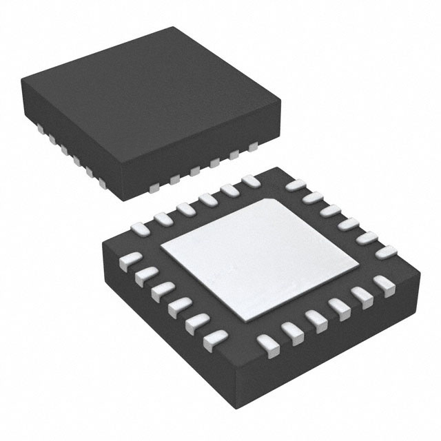
- Part No.:
- ISL6128IR
- Manufacturer:
- Renesas
- Category:
- Power Supply Controllers, Monitors
- Package:
- 24-VFQFN Exposed Pad
- Datasheet:
-
 ISL6128IR.pdf
- Description:
- IC CTRLR PWR SEQUENCE 4CH 24-QFN
- Quantity:
- Payment:

- Shipping:

Inventory:4,665
Please send an inquiry. Send us your inquiry, and we will respond immediately.
Product details
Overview
ISL6128IR from Intersil is a 4-channel power-supply sequencer with dual independent 2-channel groups, each featuring dedicated ENABLE and RESET I/O. It supports 1.5V–5.5V bias, delivers VDD+5.3V gate drive for external NFETs, provides programmable UVLO thresholds (633mV ±7mV), and enables redundant-load sequencing where a fault in one group does not affect the other. It is used in FPGA/ASIC power systems requiring isolated rail control.
For engineers reviewing the ISL6128IR datasheet, ISL6128IR pinout, ISL6128IR application, or ISL6128IR equivalent, this page delivers verified functional identity, confirmed QFN-24 package mapping, validated dual-group sequencing behavior, exact UVLO and delay timing specifications, and two manufacturer-confirmed alternative parts with documented technical and application differences.
Technical Context
The ISL6128IR implements dual independent sequencing groups (A/B and C/D), each with its own ENABLE_1/ENABLE_2 and RESET/RESET_2 signals. All four UVLO inputs must be satisfied before sequencing begins, but only the associated group's GATEs and RESET are asserted low upon a single-group UVLO fault.
Sequencing order within each group is fixed: A→B for Group 1, C→D for Group 2. Turn-on delay is set by external DLY_ON capacitors (1µA charge current to 1.266V threshold); turn-off uses identical DLY_OFF timing. Gate drive outputs deliver VDD+5.3V with 1.1µA typical turn-on current and 88mA pull-down capability during fault conditions.
Key Specifications
| Parameter | Value and Actual Design Meaning |
|---|---|
| VDD Range | 1.5V to 5.5V - supports direct bias from low-voltage rails without auxiliary LDO |
| UVLO Threshold | 633mV ±7mV - sets precise undervoltage detection point for all four monitored rails |
| Gate Drive Voltage | VDD + 5.3V - ensures full enhancement of standard logic-level NFETs across full VDD range |
| Delay Current Source | 1.0µA ±8% - defines linear ramp timing for DLY_ON/DLY_OFF pins with predictable sequence resolution |
| RESET Assertion Delay | 160ms after final GATE reaches VQP - guarantees output voltage stabilization before system release |
| Quiescent Current | 0.5mA at 5V - enables use in always-on subsystems without excessive standby loss |
| Operating Temperature | -40°C to +85°C - qualified for industrial and telecom infrastructure environments |
Pinout & Package
ISL6128IR is housed in a 24-lead 4×4 mm Pb-free QFN package (PKG DWG # L24.4x4) with exposed thermal pad (EPAD). Pin functions are electrically and physically distinct from other ISL612X variants due to dual ENABLE/RESET I/O allocation.
| Pin/Terminal | Circuit Role | Design Meaning |
|---|---|---|
| ENABLE_1 (Pin 1) | Group 1 Enable Input | Active-low signal initiating A/B sequencing; deassertion halts only Group 1 GATEs |
| ENABLE_2 (Pin 11) | Group 2 Enable Input | Active-low signal initiating C/D sequencing; independent control prevents cross-group interference |
| GATE_A (Pin 2) | Channel A Gate Driver | Drives external NFET gate with VDD+5.3V; soft-start current-limited to 1.1µA |
| GATE_B (Pin 5) | Channel B Gate Driver | Turns on after GATE_A reaches VQP; enables strict A→B ordering within Group 1 |
| GATE_C (Pin 6) | Channel C Gate Driver | First driver in Group 2; initiates C→D sequence only after both ENABLE_1 and ENABLE_2 are active |
| GATE_D (Pin 7) | Channel D Gate Driver | Turns on after GATE_C reaches VQP; completes Group 2 sequence |
| RESET (Pin 24) | Group 1 Reset Output | Open-drain output pulled low if UVLO_A/B violated or ENABLE_1 deasserted |
| RESET_2 (Pin 9) | Group 2 Reset Output | Independent open-drain output tied only to UVLO_C/D and ENABLE_2 status |
| UVLO_A–D (Pins 20,12,17,14) | Rail Monitoring Inputs | Each references internal 633mV bandgap; filtered against <30µs transients |
| DLY_ON_A–D (Pins 21,8,16,15) | Turn-On Timing Nodes | Accept external capacitor to ground; 1µA charging defines ramp delay before GATE activation |
| DLY_OFF_A–D (Pins 18,13,3,4) | Turn-Off Timing Nodes | Identical function to DLY_ON but triggered by ENABLE deassertion |
| VDD (Pin 23) | Supply Bias Input | Accepts 1.5–5.5V; powers internal charge pump and logic; regulates gate drive offset |
| GND (Pin 10) | Ground Reference | Primary return path for bias, gate drive, and monitoring circuits |
| SYSRST (Pin 22) | System Reset I/O | Open-drain bidirectional node; pulls low on any UVLO fault and propagates latch-off across daisy-chained sequencers |
Key Features
| Feature | Design Value |
|---|---|
| Dual Independent Sequencing Groups | Enables redundant power domains: failure in Group (C/D) leaves Group (A/B) fully operational with no reset propagation |
| VDD+5.3V Charge-Pump Gate Drive | Eliminates need for external high-side drivers; supports logic-level NFETs even at 1.5V VDD |
| Programmable UVLO Thresholds | 633mV reference with ±7mV tolerance allows accurate rail monitoring down to 0.7V nominal supplies |
| 160ms Post-Sequence RESET Delay | Guarantees stable output voltages before releasing downstream logic; avoids premature system boot |
| Glitch-Immune UVLO Filtering | 30µs transient rejection prevents false shutdown during brief supply disturbances |
Applications
| Graphics Card Power Management | FPGA Core & I/O Bank Sequencing |
|---|---|
Use Scenario: Dual-rail GPU core and memory interface require independent enable/disable control with fault isolation. IC Role / Device Role / Timing Role: ISL6128IR manages A/B group for GPU core (1.2V/1.8V) and C/D group for GDDR6 interface (1.35V/0.9V), enforcing strict ramp-up order and isolating faults. Use Value: Prevents GPU lockup during memory rail collapse; maintains core operation while re-initializing interface domain. | Use Scenario: High-end FPGA requires separate sequencing for core (0.85V), auxiliary (1.2V), I/O bank (1.8V), and configuration (3.3V) rails. IC Role / Device Role / Timing Role: ISL6128IR assigns core + auxiliary to Group 1 and I/O + config to Group 2, enabling independent startup and fault containment. Use Value: Allows partial reconfiguration without resetting core logic; reduces system downtime during I/O voltage anomalies. |
| Redundant Telecom Line Cards | Industrial PLC Power Subsystem |
Use Scenario: Carrier-grade line cards implement hot-swap-capable dual power feeds with automatic failover. IC Role / Device Role / Timing Role: ISL6128IR controls primary feed (Group 1) and backup feed (Group 2); monitors both independently and asserts only affected RESET. Use Value: Enables seamless switchover without resetting control plane; maintains packet forwarding during primary feed interruption. | Use Scenario: Programmable logic controller requires isolated sequencing for CPU, field I/O, communication, and analog sensor rails. IC Role / Device Role / Timing Role: ISL6128IR allocates CPU + analog to Group 1 and I/O + comms to Group 2, ensuring deterministic boot and fault localization. Use Value: Permits continued sensor data acquisition during field I/O fault; simplifies diagnostics by limiting fault scope to one group. |
Equivalent & Alternatives
The following parts are listed as comparable options for similar power-supply sequencing applications.
| Alternative Part | Technical Difference | Application Difference | Selection Advice |
|---|---|---|---|
| ISL6126IRZA | Single ENABLE input; independent per-rail turn-on based on individual UVLO satisfaction (voltage-determined), no dual-group isolation | Used when rails must power up as soon as individually valid, not in fixed groups; lacks fault containment between rails | Select ISL6126IRZA only when per-rail autonomy outweighs need for grouped redundancy |
| ISL6130IRZA | Single ENABLE; voltage-determined turn-on like ISL6126 but adds 1µA sleep mode; same QFN-24 package | Optimized for battery-backed systems needing ultra-low quiescent current; no dual-group architecture or independent RESET outputs | Choose ISL6130IRZA for portable or energy-constrained designs where group independence is unnecessary |
Compared with ISL6126IRZA and ISL6130IRZA, the ISL6128IR uniquely provides hardware-enforced fault isolation between two 2-rail domains via dedicated ENABLE/RESET pairs-enabling true redundant operation without software coordination or external logic.
Availability
ISL6128IR is available at Aetrix Electronics and suitable for graphics card power management, FPGA/ASIC supply sequencing, and redundant telecom line card applications requiring stable component supply, long-term lifecycle support, and RoHS-compliant packaging.
Supply support for ISL6128IR includes scheduled delivery planning, volume procurement assistance, BOM continuity management, traceable sourcing, and lifecycle availability coordination for OEM customers, industrial embedded developers, connected-device designers, and electronics production programs.
Manufacturer
Intersil (now part of Renesas Electronics) is a semiconductor company specializing in precision analog and power management ICs for industrial, computing, and communications markets.
The ISL6128IR belongs to the ISL612X family of multi-rail power sequencers designed specifically for complex digital systems requiring flexible, reliable, and fault-tolerant voltage sequencing-especially where redundancy and domain isolation are critical.
FAQ
What is the function of ENABLE_2 on the ISL6128IR?
ENABLE_2 (Pin 11) is the dedicated active-low enable input for the C/D channel group. When asserted low, it permits sequencing of channels C and D only after ENABLE_1 is also active and all four UVLO inputs are satisfied. Deasserting ENABLE_2 halts only Group 2 GATEs and asserts RESET_2 without affecting Group 1 operation. This enables independent control of redundant power domains in the ISL6128IR.
Does the ISL6128IR support simultaneous turn-on of both groups?
No. The ISL6128IR requires both ENABLE_1 and ENABLE_2 to be asserted low before sequencing begins, but Group A/B turns on first (after 10ms stabilization), followed by Group C/D. Simultaneous turn-on of all four rails is not supported-the device enforces strict A→B→C→D ordering within its dual-group architecture. This sequencing ensures controlled power delivery and avoids inrush current stacking in the ISL6128IR.
How does fault handling differ between the two groups in the ISL6128IR?
In the ISL6128IR, a UVLO fault on UVLO_A or UVLO_B pulls only RESET low and disables GATE_A/GATE_B; UVLO_C/D faults pull only RESET_2 low and disable GATE_C/GATE_D. Neither group's fault propagates to the other's outputs or ENABLE inputs. This hardware-level isolation eliminates need for external supervision logic and is fundamental to the ISL6128IR's redundant operation.
What is the maximum gate drive voltage the ISL6128IR can deliver?
The ISL6128IR delivers VDD + 5.3V on all GATE outputs, with VGATEh = VDD + 5.0V (for VDD < 2V) and VGATEh = VDD + 5.3V (for VDD > 2V). At VDD = 1.5V, this yields ≥6.4V gate drive-sufficient to fully enhance standard logic-level NFETs. This specification is confirmed in the Absolute Maximum Ratings and Electrical Specifications sections of the FN9005 datasheet for the ISL6128IR.
Can the ISL6128IR be used without external timing capacitors?
Yes. If no capacitor is connected to DLY_ON_A–D or DLY_OFF_A–D, the associated GATEs turn on/off immediately after the 10ms ENABLE stabilization timeout expires (for turn-on) or ENABLE deassertion (for turn-off). However, this eliminates sequencing delay-resulting in near-simultaneous switching of all four channels within a group. External capacitors are required to implement controlled ramp timing in the ISL6128IR.
ISL6128IR Specifications
- Product attributes
- Attribute value
- Manufacturer:
- Renesas
- Series:
- -
- Package/Case:
- 24-VFQFN Exposed Pad
- Packaging:
- Tube
- Product Status:
- Obsolete
- Programmable:
- Not Verified
- Applications:
- Power Supply Sequencer
- Voltage - Input:
- -
- Voltage - Supply:
- 1.5V ~ 5.5V
- Current - Supply:
- 200 µA
- Operating Temperature:
- -40°C ~ 85°C
- Grade:
- -
- Qualification:
- -
- Mounting Type:
- Surface Mount
- Supplier Device Package:
- 24-QFN (4x4)
ISL6128IR FAQ
1.How can I place an order for ISL6128IR through Aetrix?
Please submit a Request for Quotation (RFQ) for ISL6128IR on Aetrix. Our sales agent will provide a competitive quotation and guide you through the order confirmation once you accept the terms.
2.Are the price and stock information for ISL6128IR reliable?
The price and inventory of ISL6128IR are updated periodically and may fluctuate due to market conditions. Stock and pricing data are typically refreshed every 24 hours. Quotation validity for ISL6128IR is usually 5 days.
3.What payment methods are accepted for ISL6128IR?
We accept Wire Transfer, PayPal, Credit Card, Western Union, MoneyGram, and Escrow for ISL6128IR transactions.
Note: Certain payment methods may incur a processing fee.
4.How is shipping managed for ISL6128IR?
ISL6128IR orders can be shipped via leading logistics carriers, including DHL, UPS, FedEx, TNT, or Registered Mail.
Once your ISL6128IR order is processed, you will receive an email with the shipment details and tracking number.
Note: Tracking information may take up to 24 hours to appear. Express delivery typically takes 3–5 business days.
5.How can I obtain technical support or documentation for ISL6128IR?
For technical support, including ISL6128IR datasheets, pinout diagrams, or application guidance, please contact our engineering support team. They can provide detailed documentation and assistance for your ISL6128IR requirements.
6.How does Aetrix verify that ISL6128IR is sourced from the original manufacturer or authorized distributors?
All ISL6128IR products on Aetrix are procured from qualified distributors and authorized channels. Our dedicated quality assurance team conducts strict verification, including traceability checks and, if necessary, third-party testing. This ensures that ISL6128IR meets industry standards.
7.What is the process for return or replacement of ISL6128IR?
All ISL6128IR units undergo pre-shipment inspection (PSI). If there is an issue with ISL6128IR, returns or replacements are accepted under the following conditions:
1.Quantity discrepancies, incorrect items, or visible external defects (such as breakage or corrosion), acknowledged by Aetrix.
2.The issue is reported within 90 days of delivery.
3.The ISL6128IR part is unused and in its original packaging.
Return procedure for ISL6128IR:
1.Submit a request within 90 days.
2.Obtain a Return Material Authorization (RMA) from Aetrix.
ISL6128IR Tags

-
UC3845AD8TR
Texas Instruments
-
UC2843AD8TR
Texas Instruments

-
LM3880MFX-1AE/NOPB
Texas Instruments
-
LM3880MFX-1AA/NOPB
Texas Instruments
-
INA234AIYBJR
Texas Instruments

-
INA700AYWFR
Texas Instruments
-
LM3880MF-1AE/NOPB
Texas Instruments
-
LM3880MF-1AA/NOPB
Texas Instruments
-
LM3881MM/NOPB
Texas Instruments
-
UCC2802DTR
Texas Instruments
-
NCP4305DMTTWG
onsemi
-
INA237AIDGSR
Texas Instruments
Tech Hub

TTL and CMOS logic families differ in thresholds, loading, output drive, power and timing. This engineering guide compares 74HC and 74HCT, calculates noise margins and checks 3.3 V/5 V compatibility.

A practical engineering guide to 3.3V and 5V logic compatibility, input thresholds, resistor dividers, translator ICs, MOSFET level shifting, I2C pull-ups, timing limits and power-sequencing risks.

The 74HC595 uses push-pull logic outputs, while the TPIC6B595 uses 50 V open-drain DMOS sinks for higher-power loads. This guide compares timing, current limits, 3.3 V interfacing, load wiring, thermal…

The 74HC595 converts serial data into eight stable parallel outputs. This guide covers pin functions, shift and storage timing, OE and MR behavior, drive-current limits, cascading, voltage compatibilit…

A technical comparison of level-sensitive latches and edge-triggered flip-flops, covering timing windows, setup and hold limits, master–slave operation, time borrowing, race-through, HDL inference and…

A D latch stores one bit while Enable controls when data can pass. This reference covers gate-level operation, truth tables, transparency, setup and hold timing, LE versus OE, common ICs and practical …

An SR latch stores one bit through cross-coupled feedback. This engineering reference covers NOR and NAND implementations, truth tables, forbidden-state recovery, gated operation, switch debouncing, fa…

Latch circuits retain one bit through feedback. This technical reference covers SR and D latches, truth tables, transparency, timing limits, latch-versus-flip-flop behavior, applications and common log…

An engineering guide to LED driver operation, constant-current and constant-voltage outputs, linear and switching topologies, dimming, IC selection, calculations, replacement compatibility, and fault c…

Operational amplifier guide covering op amp basics, feedback, ideal vs real op amps, common configurations, buffer circuits, offset, bias current, gain-bandwidth, slew rate, rail-to-rail limits and sel…


