
 My Inquiry
 My Account


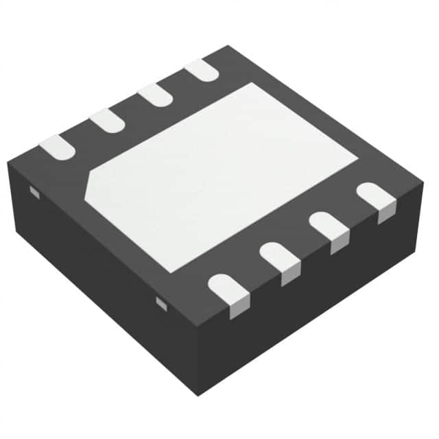
Renesas ISL6146AFRZ-T7A
- Part No.:
- ISL6146AFRZ-T7A
- Manufacturer:
- Renesas
- Category:
- OR Controllers, Ideal Diodes
- Package:
- 8-VDFN Exposed Pad
- Datasheet:
-
 ISL6146AFRZ-T7A.pdf
- Description:
- IC OR CTRLR N+1 8DFN
- Quantity:
- Payment:

- Shipping:

Inventory:1,447
Please send an inquiry. Send us your inquiry, and we will respond immediately.
Product details
Overview
ISL6146AFRZ-T7A from Renesas (formerly Intersil) is a low-voltage OR-ing FET controller designed to replace power diodes in redundant 1V–18V power distribution systems. It drives external N-channel MOSFETs with an integrated charge pump, delivers <0.3µs fast turn-off response to shorts, supports user-programmable VIN–VOUT trip point via ADJ pin, and features open-drain FAULT reporting for reverse current, gate-source/drain-source shorts, and overtemperature. Used in telecom N+1 power supplies and low-voltage processor rails.
For engineers reviewing the ISL6146AFRZ-T7A datasheet, ISL6146AFRZ-T7A pinout, ISL6146AFRZ-T7A application, or ISL6146AFRZ-T7A equivalent, this page provides verified technical context, package-validated pin functions, real-world application cards for industrial power systems, and two confirmed alternative parts with documented functional and application-level differences - all derived from FN7667 Rev 5.00 and Renesas official ordering data.
Technical Context
The ISL6146AFRZ-T7A implements dual-path fault detection: a high-speed comparator (<170ns response, 570mV typical VIN–VOUT fault threshold) triggers ~6A gate pull-down for sub-µs transients, while a slower reverse-detection path (10µs response, 57mV typical VOUT–VIN threshold) handles steady-state reverse current. Its charge pump generates gate drive up to VIN + 10.5V at 3V input and VIN + 17.5V at 12V input, enabling full enhancement of low-RDS(on) N-FETs across 1V–18V OR-ing ranges.
It uses separate BIAS (≥3V) and VIN inputs with active-high EN, distinguishing it from ISL6146B/E (active-low EN) and ISL6146C (UVLO/OVP pins). The FAULT pin reports conduction state (unlike ISL6146D/E), and ADJ pin allows resistor-programmable noise immunity (0.57–1.1V threshold with 5kΩ–100kΩ to GND).
Key Specifications
| Parameter | Value and Actual Design Meaning |
|---|---|
| VIN Range | 1V to 18V - enables OR-ing in ultra-low-voltage processor/memory rails and standard 3.3V/5V/12V telecom buses. |
| BIAS Supply | 3V to 24V independent bias - decouples controller operation from unstable or noisy OR-ing rail, ensuring reliable startup and regulation. |
| Fast Turn-off Time | 65–130ns - isolates faulty supply within one switching cycle, preventing bus collapse during catastrophic VIN short. |
| GATE Drive Voltage | VIN + 7V (at VIN = 3.3V) to VIN + 17.5V (at VIN = 12V) - ensures robust N-FET enhancement even at lowest input voltages. |
| VIN–VOUT Fault Threshold | 330–570mV (programmable via ADJ) - adjustable sensitivity prevents false trips due to IR drop or load transients. |
| FAULT Sink Current | 5–9mA - sufficient to drive optocoupler inputs or microcontroller interrupt lines without external buffering. |
| Operating Temp | –40°C to +125°C - qualified for industrial and telecom base station environments with extended thermal margins. |
Pinout & Package
ISL6146AFRZ-T7A is housed in an 8-lead 3×3mm DFN package (Pb-free, RoHS-compliant, thermal pad connected to GND). The exposed pad improves thermal performance (θJC = 5°C/W) and must be soldered to PCB ground plane.
| Pin/Terminal | Circuit Role | Design Meaning |
|---|---|---|
| GATE | Charge-pump-driven gate driver output | Delivers up to 6A pulsed sink current to rapidly turn off external N-FET during reverse faults; voltage swings up to VIN + 17.5V. |
| VIN | Sourcing supply sense input | Monitors OR-ing FET source node; initiates turn-off when VIN falls below VOUT by programmed ADJ threshold. |
| BIAS | Independent bias supply input | Provides stable ≥3V power for internal circuitry and charge pump - remains functional even if VIN sags below 1V. |
| EN | Active-high enable input | Pulled low internally (2MΩ); asserts GATE only when logic-high signal applied - enables system-level sequencing control. |
| GND | Ground reference | Common return for all analog and digital blocks; connects to thermal pad for optimal heat dissipation. |
| FAULT | Open-drain fault indicator | Asserts low on GATE-VIN overvoltage, VIN-VOUT > 570mV, FET terminal shorts, or overtemperature (>150°C). |
| ADJ | VIN–VOUT threshold programming node | Accepts 5kΩ–100kΩ resistor to GND to set noise-immunity trip point from 0.57V to 1.1V - critical for high-current bus stability. |
| VOUT | Load-side sense input | Connects to common power bus; compared against VIN to detect reverse current flow and initiate FET turn-off. |
Key Features
| Feature | Design Value |
|---|---|
| Integrated charge pump | Eliminates need for external high-side gate driver IC or bootstrap capacitor - reduces BOM count and layout complexity in compact OR-ing designs. |
| Programmable VIN–VOUT trip point | Enables precise tuning of fault sensitivity to match actual system IR drop and transient behavior - avoids nuisance shutdowns in high-current 12V/48V backplanes. |
| High-speed comparator with 6A gate sink | Guarantees <130ns FET turn-off during catastrophic VIN failure - protects shared bus from single-point supply collapse in N+1 architectures. |
| Conduction-state reporting via FAULT | Distinguishes between disabled state (EN = low) and active fault conditions (e.g., G-S short), enabling diagnostic logging in mission-critical power systems. |
| Separate BIAS and VIN inputs | Allows use of clean auxiliary rail (e.g., 5V standby) to power controller while OR-ing unregulated 12V main rail - improves reliability during brownout events. |
Applications
| N+1 Telecom Power Distribution | Industrial Uninterruptible Power Supply (UPS) |
|---|---|
|
Use Scenario: Dual 12V DC power feeds from separate rectifiers feed a common 12V bus powering baseband processing units. IC Role / Device Role / Timing Role: ISL6146AFRZ-T7A controls parallel N-FETs to enable automatic current sharing and isolate failed supply within 130ns. Use Value: Replaces 0.5V-drop Schottky diodes, cutting conduction loss by >80% at 30A and eliminating thermal runaway risk in enclosed chassis. |
Use Scenario: 48V battery backup and AC/DC converter feed same load bus in factory automation PLCs. IC Role / Device Role / Timing Role: ISL6146AFRZ-T7A monitors VOUT–VIN differential to detect battery reversal or converter failure and disable faulty path. Use Value: Prevents reverse discharge of healthy battery into failed converter, extending backup runtime and avoiding fire hazard. |
| Low-Voltage Server Memory Rail | Storage System Redundant 3.3V Supply |
|
Use Scenario: Two 1.2V DDR5 memory regulator outputs feed shared DIMM VDDQ rail with tight voltage tolerance. IC Role / Device Role / Timing Role: ISL6146AFRZ-T7A operates down to 1V with 3V BIAS, enabling OR-ing at core memory voltage levels. Use Value: Maintains <±10mV bus regulation during hot-swap events, preventing memory corruption during live module replacement. |
Use Scenario: Dual 3.3V LDOs power SAS controller ASIC in enterprise SSD enclosures with thermal constraints. IC Role / Device Role / Timing Role: ISL6146AFRZ-T7A's ADJ pin sets 0.8V trip threshold to tolerate 50mV IR drop across 2oz copper traces. Use Value: Avoids false tripping during 5A load steps while ensuring sub-100ns isolation if one LDO fails short. |
Equivalent & Alternatives
The following parts are listed as comparable options for similar OR-ing FET controller applications.
| Alternative Part | Technical Difference | Application Difference | Selection Advice |
|---|---|---|---|
| ISL6146BFUZ | Active-low EN instead of active-high; identical BIAS/VIN separation, FAULT reporting, and ADJ programmability. | Requires inverted enable signal from host controller; otherwise drop-in compatible in same PCB footprint (MSOP-8). | Select when system enable logic is active-low or when consolidating BOM across multiple ISL6146 variants. |
| TPS2410PWR | No separate BIAS pin; powered from VDD (tied to VIN); lacks ADJ-programmable threshold - fixed ~100mV reverse detection. | Cannot operate below 2.5V VIN; unsuitable for 1V–2V memory rails; simpler layout but lower noise immunity in high-current systems. | Choose for cost-sensitive 3.3V/5V applications where BIAS independence and fine threshold tuning are not required. |
Compared with ISL6146BFUZ, ISL6146AFRZ-T7A offers active-high sequencing control and DFN packaging for higher power density; versus TPS2410PWR, it delivers true 1V operation, programmable noise margin, and superior fault diagnostics - critical for high-reliability telecom and server platforms.
Availability
ISL6146AFRZ-T7A is available at Aetrix Electronics and suitable for N+1 telecom power distribution, industrial UPS systems, and low-voltage server memory rails requiring stable component supply, long-term lifecycle support, and RoHS-compliant DFN packaging.
Supply support for ISL6146AFRZ-T7A includes scheduled delivery planning, volume procurement assistance, BOM continuity management, traceable sourcing, and lifecycle availability coordination for OEM customers, industrial embedded developers, connected-device designers, and electronics production programs.
Manufacturer
Renesas Electronics Corporation, formed from the merger of Intersil and IDT, is a global semiconductor leader specializing in microcontrollers, analog power, and connectivity solutions for industrial, automotive, and infrastructure markets.
The ISL6146AFRZ-T7A belongs to Renesas' high-efficiency power OR-ing controller product line, engineered specifically to replace lossy diodes in redundant 1V–18V power systems while delivering sub-130ns fault response and diagnostic FAULT signaling.
FAQ
What is the minimum operating voltage for ISL6146AFRZ-T7A?
The ISL6146AFRZ-T7A supports OR-ing down to 1V on the VIN rail when supplied with a separate ≥3V BIAS voltage. This enables use in ultra-low-voltage applications such as DDR5 memory VDDQ rails and advanced SoC core supplies where traditional diode-based OR-ing would incur prohibitive conduction losses.
Does ISL6146AFRZ-T7A require an external gate driver?
No. The ISL6146AFRZ-T7A integrates a fully self-contained charge pump that generates gate drive up to VIN + 17.5V, eliminating the need for external high-side drivers or bootstrap components. This simplifies design and reduces board space in compact OR-ing implementations using discrete N-channel MOSFETs.
How does the ADJ pin affect fault sensitivity in ISL6146AFRZ-T7A?
The ADJ pin on ISL6146AFRZ-T7A accepts a resistor to GND (5kΩ–100kΩ) to set the VIN–VOUT voltage threshold from 0.57V to 1.1V. This programmability allows designers to tune noise immunity - for example, selecting 100kΩ raises the trip point to avoid false shutdowns caused by IR drop across high-current PCB traces.
What fault conditions does the FAULT pin of ISL6146AFRZ-T7A report?
The FAULT pin on ISL6146AFRZ-T7A asserts low for six confirmed conditions: VIN–VOUT > 570mV (forward fault), GATE–VIN > 440mV (gate-source short), VOUT > VIN (reverse current), thermal shutdown (>150°C), BIAS undervoltage, and EN deassertion. Unlike ISL6146D/E, it reports conduction state, enabling precise fault diagnosis.
Is ISL6146AFRZ-T7A pin-compatible with other ISL6146 variants?
Yes - ISL6146AFRZ-T7A shares identical 8-lead DFN (3×3mm) pinout and function mapping with ISL6146BFRZ, ISL6146CFRZ, ISL6146DFRZ, and ISL6146EFRZ. However, EN polarity (active-high vs. active-low) and FAULT reporting capability differ; firmware or enable logic must be verified before substitution.
ISL6146AFRZ-T7A Specifications
- Product attributes
- Attribute value
- Manufacturer:
- Renesas
- Series:
- -
- Package/Case:
- 8-VDFN Exposed Pad
- Packaging:
- Tape & Reel (TR)
- Product Status:
- Obsolete
- Type:
- N+1 ORing Controller
- FET Type:
- N-Channel
- Ratio - Input:Output:
- N:1
- Internal Switch(s):
- No
- Delay Time - ON:
- -
- Delay Time - OFF:
- 65 ns
- Current - Output (Max):
- -
- Current - Supply:
- 25 µA
- Voltage - Supply:
- 3V ~ 20V
- Applications:
- N+1 Power Supplies, Telecom/Datacom Systems
- Operating Temperature:
- -40°C ~ 125°C
- Grade:
- -
- Qualification:
- -
- Mounting Type:
- Surface Mount
- Supplier Device Package:
- 8-DFN (3x3)
ISL6146AFRZ-T7A FAQ
1.How can I place an order for ISL6146AFRZ-T7A through Aetrix?
Please submit a Request for Quotation (RFQ) for ISL6146AFRZ-T7A on Aetrix. Our sales agent will provide a competitive quotation and guide you through the order confirmation once you accept the terms.
2.Are the price and stock information for ISL6146AFRZ-T7A reliable?
The price and inventory of ISL6146AFRZ-T7A are updated periodically and may fluctuate due to market conditions. Stock and pricing data are typically refreshed every 24 hours. Quotation validity for ISL6146AFRZ-T7A is usually 5 days.
3.What payment methods are accepted for ISL6146AFRZ-T7A?
We accept Wire Transfer, PayPal, Credit Card, Western Union, MoneyGram, and Escrow for ISL6146AFRZ-T7A transactions.
Note: Certain payment methods may incur a processing fee.
4.How is shipping managed for ISL6146AFRZ-T7A?
ISL6146AFRZ-T7A orders can be shipped via leading logistics carriers, including DHL, UPS, FedEx, TNT, or Registered Mail.
Once your ISL6146AFRZ-T7A order is processed, you will receive an email with the shipment details and tracking number.
Note: Tracking information may take up to 24 hours to appear. Express delivery typically takes 3–5 business days.
5.How can I obtain technical support or documentation for ISL6146AFRZ-T7A?
For technical support, including ISL6146AFRZ-T7A datasheets, pinout diagrams, or application guidance, please contact our engineering support team. They can provide detailed documentation and assistance for your ISL6146AFRZ-T7A requirements.
6.How does Aetrix verify that ISL6146AFRZ-T7A is sourced from the original manufacturer or authorized distributors?
All ISL6146AFRZ-T7A products on Aetrix are procured from qualified distributors and authorized channels. Our dedicated quality assurance team conducts strict verification, including traceability checks and, if necessary, third-party testing. This ensures that ISL6146AFRZ-T7A meets industry standards.
7.What is the process for return or replacement of ISL6146AFRZ-T7A?
All ISL6146AFRZ-T7A units undergo pre-shipment inspection (PSI). If there is an issue with ISL6146AFRZ-T7A, returns or replacements are accepted under the following conditions:
1.Quantity discrepancies, incorrect items, or visible external defects (such as breakage or corrosion), acknowledged by Aetrix.
2.The issue is reported within 90 days of delivery.
3.The ISL6146AFRZ-T7A part is unused and in its original packaging.
Return procedure for ISL6146AFRZ-T7A:
1.Submit a request within 90 days.
2.Obtain a Return Material Authorization (RMA) from Aetrix.
ISL6146AFRZ-T7A Tags

-
LM66100DCKR
Texas Instruments
-
LM66200DRLR
Texas Instruments
-
LM66100DCKT
Texas Instruments

-
AP74700QW6-7
Diodes Incorporated
-
LM73100RPWR
Texas Instruments
-
LM74502DDFR
Texas Instruments
-
LM74700QDBVRQ1
Texas Instruments
-
MAX40200AUK+T
Analog Devices Inc./Maxim Integrated
-
MAX40200ANS+T
Analog Devices Inc./Maxim Integrated
-
MAX40203AUK+T
Analog Devices Inc./Maxim Integrated
-
MAX40203ANS+T
Analog Devices Inc./Maxim Integrated
-
LM74502QDDFRQ1
Texas Instruments
Tech Hub

TTL and CMOS logic families differ in thresholds, loading, output drive, power and timing. This engineering guide compares 74HC and 74HCT, calculates noise margins and checks 3.3 V/5 V compatibility.

A practical engineering guide to 3.3V and 5V logic compatibility, input thresholds, resistor dividers, translator ICs, MOSFET level shifting, I2C pull-ups, timing limits and power-sequencing risks.

The 74HC595 uses push-pull logic outputs, while the TPIC6B595 uses 50 V open-drain DMOS sinks for higher-power loads. This guide compares timing, current limits, 3.3 V interfacing, load wiring, thermal…

The 74HC595 converts serial data into eight stable parallel outputs. This guide covers pin functions, shift and storage timing, OE and MR behavior, drive-current limits, cascading, voltage compatibilit…

A technical comparison of level-sensitive latches and edge-triggered flip-flops, covering timing windows, setup and hold limits, master–slave operation, time borrowing, race-through, HDL inference and…

A D latch stores one bit while Enable controls when data can pass. This reference covers gate-level operation, truth tables, transparency, setup and hold timing, LE versus OE, common ICs and practical …

An SR latch stores one bit through cross-coupled feedback. This engineering reference covers NOR and NAND implementations, truth tables, forbidden-state recovery, gated operation, switch debouncing, fa…

Latch circuits retain one bit through feedback. This technical reference covers SR and D latches, truth tables, transparency, timing limits, latch-versus-flip-flop behavior, applications and common log…

An engineering guide to LED driver operation, constant-current and constant-voltage outputs, linear and switching topologies, dimming, IC selection, calculations, replacement compatibility, and fault c…

Operational amplifier guide covering op amp basics, feedback, ideal vs real op amps, common configurations, buffer circuits, offset, bias current, gain-bandwidth, slew rate, rail-to-rail limits and sel…


