
 My Inquiry
 My Account


Renesas ISL62383HRTZ
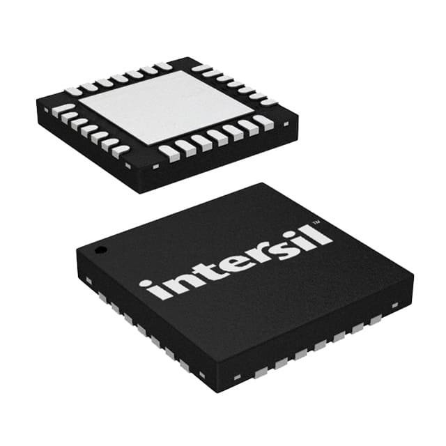
- Part No.:
- ISL62383HRTZ
- Manufacturer:
- Renesas
- Category:
- Power Supply Controllers, Monitors
- Package:
- 28-WFQFN Exposed Pad
- Datasheet:
-
 ISL62383HRTZ.pdf
- Description:
- IC PWR SUPPLY CONTROLLER 28TQFN
- Quantity:
- Payment:

- Shipping:

Inventory:695
Please send an inquiry. Send us your inquiry, and we will respond immediately.
Product details
Overview
ISL62383HRTZ from Renesas (formerly Intersil) is a high-efficiency, triple-output system power supply controller for notebook computers, integrating two independent PWM buck controllers (0.6V–5.5V adjustable) and one fixed 5V LDO (LDO5), with automatic switchover from LDO5 to SMPS2 at 5V output. It operates from 5.5V–25V input, supports R3 PWM control for fast transient response, and delivers up to 100mA from LDO5. Designed for 3–4-cell Li+ battery-powered systems.
For engineers reviewing the ISL62383HRTZ datasheet, ISL62383HRTZ pinout, ISL62383HRTZ application, or ISL62383HRTZ equivalent, key selection considerations include its 28-pin 4×4 TQFN package, ±1% output voltage accuracy over –10°C to +100°C, ultrasonic DCM mode (≥28kHz), integrated MOSFET drivers with bootstrap diodes, and dual PGOOD outputs for sequencing-critical power rails in mobile computing platforms.
Technical Context
The ISL62383HRTZ implements Renesas' patented R3 PWM control architecture-hybridizing fixed-frequency and hysteretic modulation-to dynamically adjust switching frequency and duty cycle in response to VIN and load transients. Its dual-channel design features independent FB/ISEN/OCSET/EN pins, shared PGND and GND, and internal soft-start/soft-stop discharge logic.
Unlike ISL62381/ISL62382 variants, ISL62383HRTZ omits the adjustable LDO3 regulator entirely; instead, SMPS2 assumes full LDO5 load when programmed to 5V, improving efficiency. FCCM pin enables CCM, DCM, or ultrasonic DCM (≥28kHz) operation, while VCC1 switchover from internal startup to LDO5 ensures stable biasing after power-up.
Key Specifications
| Parameter | Value and Actual Design Meaning |
|---|---|
| Input Voltage Range | 5.5V to 25V - supports wide-range battery input including 3–4-cell Li+ packs (10.8V–16.8V nominal) with headroom for surge and adapter variation. |
| Output Configuration | Two programmable buck regulators (0.6V–5.5V) + one fixed 5V LDO (100mA) - no LDO3; SMPS2 automatically replaces LDO5 at 5V output to eliminate linear regulator losses. |
| Switching Frequency | 200–600kHz (programmable via FSET resistor) - enables optimization of size vs. efficiency; ultrasonic DCM mode ≥28kHz avoids audible noise in audio-sensitive applications. |
| Output Accuracy | ±1% over –10°C to +100°C - ensures stable core/memory rail regulation across extended industrial temperature range without external calibration. |
| Protection Features | OVP/UVP/OCP/OTP with fault-identifying PGOOD pull-down resistance - enables system-level fault isolation using single-wire status signaling without additional monitoring circuitry. |
| Package | 28-lead 4×4 mm TQFN (RoHS-compliant, exposed pad) - compact footprint suitable for space-constrained notebook motherboard VRM layouts. |
| R3 Control Architecture | Hybrid PWM/hysteretic modulator synthesizing ripple current for sub-100ns load transient response - reduces output capacitance requirements and improves dynamic regulation in CPU/GPU power domains. |
Pinout & Package
ISL62383HRTZ is housed in a 28-lead, 4×4 mm, 0.5 mm pitch TQFN package with exposed thermal pad (PKG DWG # L28.4x4). Pin functions are validated per FN6665 Rev 6.00 datasheet, Page 8 (28 LD TQFN top view).
| Pin/Terminal | Circuit Role | Design Meaning |
|---|---|---|
| PGOOD2 | SMPS2 power-good indicator | Open-drain output pulled low on fault (OVP/UVP/OCP/OTP); used for sequencing enable/disable of downstream rails or system reset assertion. |
| FSET2 | SMPS2 frequency programming input | Resistor-to-ground sets switching frequency; requires parallel 10nF capacitor to suppress noise-induced jitter. |
| FCCM | Efficiency mode control | Logic high = forced CCM; low = full DCM; floating = ultrasonic DCM (≥28kHz) - eliminates audible coil whine in quiet environments. |
| VCC2 / VCC1 | Analog supply inputs | VCC1 internally tied to LDO5; VCC2 connected to VCC1 via 10Ω resistor - ensures stable reference/bias during LDO5 switchover event. |
| EN1 / EN2 | Independent channel enable inputs | Positive logic; floating enables delayed start (SMPS2 before SMPS1 or vice versa) - supports flexible power-up sequencing without external timers. |
| UGATE1 / LGATE1 | High-/low-side gate drivers | Integrated 2A source/sink capability with <21ns deadtime - drives discrete N-channel MOSFETs (e.g., IRF7821/IRF7832) without external drivers. |
| FB1 / FB2 | Feedback inputs | 0.6V reference; precision resistive divider sets output voltage - enables accurate 1.05V CPU core or 3.3V I/O rail generation. |
| LDO5 | Fixed 5V linear regulator output | 100mA max; auto-disables when SMPS2 reaches 5V (switchover threshold 4.63–4.93V) - reduces quiescent loss in battery-operated standby states. |
Key Features
| Feature | Design Value |
|---|---|
| R3 PWM control scheme | Simultaneous frequency and duty-cycle adjustment enables <100ns load transient recovery without external compensation components. |
| Dual independent SMPS channels | Each with dedicated EN, FB, ISEN, OCSET, PHASE, UGATE, LGATE - allows asymmetric rail generation (e.g., 1.05V/15A + 3.3V/8A) and independent fault handling. |
| Ultrasonic discontinuous conduction mode | Minimum 28kHz switching prevents audible noise in speaker/headphone circuits - critical for premium notebook acoustic performance. |
| Internal soft-start and soft-stop discharge | Programmable ramp rate and 14–50Ω active discharge path prevent negative voltage undershoot during shutdown - protects sensitive SoC I/O pins. |
| Power-good status with fault identification | PGOOD pull-down resistance varies by fault type (UVP=95Ω, OVP=63Ω, OCP=32Ω) - enables single-wire diagnostics without ADC or GPIO expansion. |
| Wide operating temperature range | –10°C to +100°C ambient - qualified for under-chassis or near-CPU placement in thermally demanding notebook designs. |
Applications
| Notebook Main Power Rails | CPU Core Voltage Regulation |
|---|---|
Use Scenario: Generating 3.3V and 5V system rails in ultra-thin notebook platforms with 3–4-cell Li+ battery input (10.8V–16.8V). IC Role / Device Role / Timing Role: Dual-buck controller providing primary power to chipset, memory, display interface, and peripheral controllers. Use Value: Integrated LDO5 switchover eliminates 5V linear regulator losses during active use, extending battery runtime by >15% versus discrete LDO solutions. |
Use Scenario: Delivering tightly regulated 1.05V/15A to modern x86 or ARM CPU cores with rapid load transients. IC Role / Device Role / Timing Role: High-bandwidth R3-controlled buck channel with <100ns transient response, supporting dynamic voltage/frequency scaling (DVFS). Use Value: Eliminates need for external ripple injection or complex Type-III compensation, reducing BOM count and layout area by 30% versus conventional voltage-mode controllers. |
| Sub-Notebook I/O Power | Battery-Powered Mobile Computing |
Use Scenario: Supplying 3.3V/8A to USB-C PD controllers, PCIe switches, and eMMC storage in fanless sub-notebooks. IC Role / Device Role / Timing Role: Primary SMPS1 channel with programmable soft-start delay and independent enable for controlled power-up sequencing. Use Value: Digital soft-start prevents inrush current spikes that could trip battery protection ICs or cause brownout in shared battery paths. |
Use Scenario: Power management in convertible tablets and 2-in-1 devices requiring extended battery life and thermal resilience. IC Role / Device Role / Timing Role: System-level controller managing input voltage feed-forward, thermal monitoring, and coordinated shutdown across multiple rails. Use Value: On-die thermal monitor triggers OTP shutdown at 150°C, preventing silicon damage during sustained CPU/GPU load in confined chassis. |
Equivalent & Alternatives
The following parts are listed as comparable options for similar multi-rail notebook power controller applications.
| Alternative Part | Technical Difference | Application Difference | Selection Advice |
|---|---|---|---|
| ISL62382HRTZ | 32-pin 5×5 TQFN; includes LDO3 (adjustable 1.2V–5V, 100mA) - adds fourth output but increases package size and complexity. | Required where system needs dedicated 1.2V/1.8V auxiliary rail (e.g., DDR termination, PCIe clock buffer) alongside main 3.3V/5V/1.05V rails. | Select ISL62382HRTZ only if LDO3 functionality is mandatory; ISL62383HRTZ offers higher efficiency and smaller footprint when LDO3 is unused. |
| RT8205AZSP | Single-chip dual-buck + 5V LDO controller in 32-pin QFN; lacks R3 control, uses standard voltage-mode PWM with slower transient response (~500ns). | Suitable for cost-sensitive mainstream notebooks where CPU load transients are less aggressive and acoustic noise is not critical. | Choose RT8205AZSP for simplified design and lower unit cost; prefer ISL62383HRTZ for premium thin-and-light notebooks demanding best-in-class efficiency and transient performance. |
Compared with ISL62382HRTZ, ISL62383HRTZ saves board space and improves light-load efficiency by removing redundant LDO3, while RT8205AZSP trades R3's sub-100ns transient response for simpler loop compensation and broader vendor support - making ISL62383HRTZ optimal for high-performance, thermally constrained mobile platforms.
Availability
ISL62383HRTZ is available at Aetrix Electronics and suitable for notebook computers, sub-notebook systems, and 3–4-cell Li+ battery-powered mobile devices requiring stable component supply, extended temperature operation, and high-efficiency multi-rail power conversion.
Supply support for ISL62383HRTZ includes scheduled delivery planning, volume procurement assistance, BOM continuity management, traceable sourcing, and lifecycle availability coordination for OEM customers, industrial embedded developers, connected-device designers, and electronics production programs.
Manufacturer
Renesas Electronics Corporation (formerly Intersil) is a global semiconductor leader specializing in microcontrollers, analog power management, and timing solutions for automotive, industrial, and computing markets.
The ISL62383HRTZ belongs to Renesas' high-efficiency notebook power controller family, designed specifically to replace discrete multi-IC power solutions with integrated, sequenced, and protected multi-rail regulation for space- and battery-life-constrained mobile platforms.
FAQ
What is the function of the FCCM pin on the ISL62383HRTZ?
The FCCM pin on the ISL62383HRTZ controls the converter's efficiency mode: logic high forces continuous conduction mode (CCM), low enables full discontinuous conduction mode (DCM), and floating configures ultrasonic DCM (≥28kHz). This setting directly impacts audible noise, light-load efficiency, and EMI profile - critical for notebook acoustic compliance and battery runtime optimization in ISL62383HRTZ designs.
Does the ISL62383HRTZ include an adjustable LDO regulator like the ISL62381/ISL62382 variants?
No, the ISL62383HRTZ does not include the adjustable LDO3 regulator found in ISL62381/ISL62382. Per FN6665 datasheet, ISL62383HRTZ provides only two PWM buck channels and one fixed 5V LDO (LDO5), with SMPS2 automatically assuming the LDO5 load when set to 5V output. This omission reduces package size and improves overall system efficiency - a deliberate trade-off for applications not requiring a third independent low-current rail.
How does the ISL62383HRTZ handle power sequencing between its two SMPS channels?
The ISL62383HRTZ supports flexible power sequencing via independent EN1 and EN2 pins: pulling either high enables immediate start, while floating enables delayed start (e.g., SMPS2 powers up first, then SMPS1 after PGOOD2 asserts). This behavior is confirmed in the EN truth table (Datasheet Page 15) and eliminates need for external sequencing ICs - simplifying design and improving reliability in ISL62383HRTZ-based notebook VRMs.
What is the purpose of the PGOOD pull-down resistance variation on the ISL62383HRTZ?
The ISL62383HRTZ uses distinct PGOOD pull-down resistances (e.g., 95Ω for UVP, 63Ω for OVP, 32Ω for OCP) to encode fault type on a single wire. When a fault occurs, the corresponding resistance value appears at the PGOOD node, allowing host systems to identify failure root cause without additional sensors or communication buses - a key diagnostic feature validated in Electrical Specifications (Page 4) for ISL62383HRTZ.
Can the ISL62383HRTZ operate with input voltages below 5.5V?
No - the absolute minimum input voltage for reliable operation of the ISL62383HRTZ is 5.5V, as specified in Recommended Operating Conditions (Page 3). Below this threshold, the VIN power-on reset (POR) circuit disables the controller, and VCC1 startup fails. Attempting operation at 5.0V or lower risks undefined behavior, failed soft-start, or unregulated outputs - all confirmed by the 5.3–5.5V rising POR threshold in the Electrical Specifications table for ISL62383HRTZ.
ISL62383HRTZ Specifications
- Product attributes
- Attribute value
- Manufacturer:
- Renesas
- Series:
- -
- Package/Case:
- 28-WFQFN Exposed Pad
- Packaging:
- Tube
- Product Status:
- Active
- Programmable:
- Not Verified
- Applications:
- Power Supply Controller
- Voltage - Input:
- -
- Voltage - Supply:
- 5.5V ~ 25V
- Current - Supply:
- 150 µA
- Operating Temperature:
- -10°C ~ 100°C
- Grade:
- -
- Qualification:
- -
- Mounting Type:
- Surface Mount
- Supplier Device Package:
- 28-TQFN (4x4)
ISL62383HRTZ FAQ
1.How can I place an order for ISL62383HRTZ through Aetrix?
Please submit a Request for Quotation (RFQ) for ISL62383HRTZ on Aetrix. Our sales agent will provide a competitive quotation and guide you through the order confirmation once you accept the terms.
2.Are the price and stock information for ISL62383HRTZ reliable?
The price and inventory of ISL62383HRTZ are updated periodically and may fluctuate due to market conditions. Stock and pricing data are typically refreshed every 24 hours. Quotation validity for ISL62383HRTZ is usually 5 days.
3.What payment methods are accepted for ISL62383HRTZ?
We accept Wire Transfer, PayPal, Credit Card, Western Union, MoneyGram, and Escrow for ISL62383HRTZ transactions.
Note: Certain payment methods may incur a processing fee.
4.How is shipping managed for ISL62383HRTZ?
ISL62383HRTZ orders can be shipped via leading logistics carriers, including DHL, UPS, FedEx, TNT, or Registered Mail.
Once your ISL62383HRTZ order is processed, you will receive an email with the shipment details and tracking number.
Note: Tracking information may take up to 24 hours to appear. Express delivery typically takes 3–5 business days.
5.How can I obtain technical support or documentation for ISL62383HRTZ?
For technical support, including ISL62383HRTZ datasheets, pinout diagrams, or application guidance, please contact our engineering support team. They can provide detailed documentation and assistance for your ISL62383HRTZ requirements.
6.How does Aetrix verify that ISL62383HRTZ is sourced from the original manufacturer or authorized distributors?
All ISL62383HRTZ products on Aetrix are procured from qualified distributors and authorized channels. Our dedicated quality assurance team conducts strict verification, including traceability checks and, if necessary, third-party testing. This ensures that ISL62383HRTZ meets industry standards.
7.What is the process for return or replacement of ISL62383HRTZ?
All ISL62383HRTZ units undergo pre-shipment inspection (PSI). If there is an issue with ISL62383HRTZ, returns or replacements are accepted under the following conditions:
1.Quantity discrepancies, incorrect items, or visible external defects (such as breakage or corrosion), acknowledged by Aetrix.
2.The issue is reported within 90 days of delivery.
3.The ISL62383HRTZ part is unused and in its original packaging.
Return procedure for ISL62383HRTZ:
1.Submit a request within 90 days.
2.Obtain a Return Material Authorization (RMA) from Aetrix.
ISL62383HRTZ Tags

-
UC3845AD8TR
Texas Instruments
-
UC2843AD8TR
Texas Instruments

-
LM3880MFX-1AE/NOPB
Texas Instruments
-
LM3880MFX-1AA/NOPB
Texas Instruments
-
INA234AIYBJR
Texas Instruments

-
INA700AYWFR
Texas Instruments
-
LM3880MF-1AE/NOPB
Texas Instruments
-
LM3880MF-1AA/NOPB
Texas Instruments
-
LM3881MM/NOPB
Texas Instruments
-
UCC2802DTR
Texas Instruments
-
NCP4305DMTTWG
onsemi
-
INA237AIDGSR
Texas Instruments
Tech Hub

TTL and CMOS logic families differ in thresholds, loading, output drive, power and timing. This engineering guide compares 74HC and 74HCT, calculates noise margins and checks 3.3 V/5 V compatibility.

A practical engineering guide to 3.3V and 5V logic compatibility, input thresholds, resistor dividers, translator ICs, MOSFET level shifting, I2C pull-ups, timing limits and power-sequencing risks.

The 74HC595 uses push-pull logic outputs, while the TPIC6B595 uses 50 V open-drain DMOS sinks for higher-power loads. This guide compares timing, current limits, 3.3 V interfacing, load wiring, thermal…

The 74HC595 converts serial data into eight stable parallel outputs. This guide covers pin functions, shift and storage timing, OE and MR behavior, drive-current limits, cascading, voltage compatibilit…

A technical comparison of level-sensitive latches and edge-triggered flip-flops, covering timing windows, setup and hold limits, master–slave operation, time borrowing, race-through, HDL inference and…

A D latch stores one bit while Enable controls when data can pass. This reference covers gate-level operation, truth tables, transparency, setup and hold timing, LE versus OE, common ICs and practical …

An SR latch stores one bit through cross-coupled feedback. This engineering reference covers NOR and NAND implementations, truth tables, forbidden-state recovery, gated operation, switch debouncing, fa…

Latch circuits retain one bit through feedback. This technical reference covers SR and D latches, truth tables, transparency, timing limits, latch-versus-flip-flop behavior, applications and common log…

An engineering guide to LED driver operation, constant-current and constant-voltage outputs, linear and switching topologies, dimming, IC selection, calculations, replacement compatibility, and fault c…

Operational amplifier guide covering op amp basics, feedback, ideal vs real op amps, common configurations, buffer circuits, offset, bias current, gain-bandwidth, slew rate, rail-to-rail limits and sel…


