
 My Inquiry
 My Account


Renesas ISL6265CHRTZ
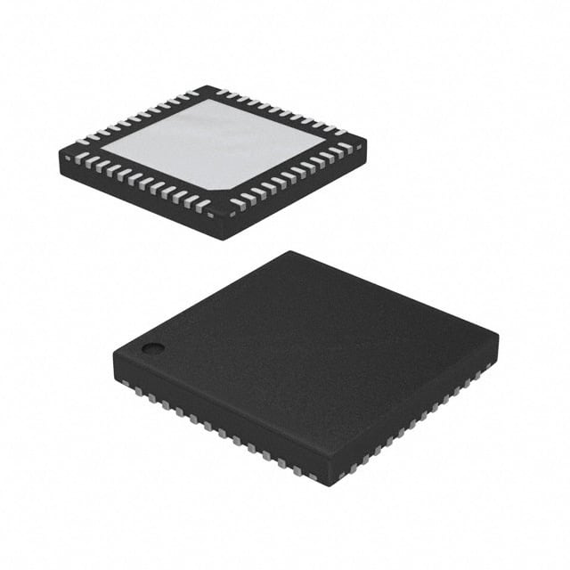
- Part No.:
- ISL6265CHRTZ
- Manufacturer:
- Renesas
- Category:
- Special Purpose Regulators
- Package:
- 48-WFQFN Exposed Pad
- Datasheet:
-
 ISL6265CHRTZ.pdf
- Description:
- IC REG CTRLR AMD 3OUT 48TQFN
- Quantity:
- Payment:

- Shipping:

Inventory:3,928
Please send an inquiry. Send us your inquiry, and we will respond immediately.
Product details
Overview
ISL6265CHRTZ from Renesas (formerly Intersil) is a multi-output voltage regulator controller IC designed for AMD SVI-capable mobile CPUs, integrating three independent PWM controllers with embedded 2A MOSFET gate drivers. It supports dual-plane (VDD0/VDD1) or uniplane two-phase core regulation plus dedicated Northbridge (VDDNB) control, delivers 0.5% system voltage accuracy over temperature, and operates across 6–24V input with programmable 200–500kHz switching frequency.
For engineers reviewing the ISL6265CHRTZ datasheet, ISL6265CHRTZ pinout, ISL6265CHRTZ application, or ISL6265CHRTZ equivalent, this page provides verified technical context on R3 Technology™ modulator performance, SVI interface timing, differential remote sensing implementation, DCR/rDS(ON) current sensing architecture, and thermal design constraints for AMD Griffin platform notebook power delivery.
Technical Context
The ISL6265CHRTZ implements Renesas' patented R3 Technology™ modulator, enabling variable-frequency response during load transients for faster regulation than fixed-frequency buck controllers. Its three-channel architecture supports flexible configuration: either two independent single-phase core outputs (VDD0/VDD1) with Northbridge (VDDNB), or interleaved two-phase core + VDDNB - all with per-channel overvoltage, undervoltage, and overcurrent protection.
Core and Northbridge outputs use separate feedback paths with unity-gain differential amplifiers for remote CPU die sensing, while current sensing employs lossless inductor DCR for core channels and rDS(ON) sensing for Northbridge. The Serial VID (SVI) interface operates as a two-wire I²C-compatible bus supporting 12.5mV voltage steps from 0.500V to 1.55V and PSI_L power-saving mode coordination.
Key Specifications
| Parameter | Value and Actual Design Meaning |
|---|---|
| Output Configuration | Three independent PWM channels: dual single-phase core (VDD0/VDD1) + Northbridge (VDDNB), or uniplane two-phase core + VDDNB |
| Voltage Accuracy | ±0.5% system accuracy over –10°C to +100°C ambient for core/NB outputs within 0.75–1.55V range |
| SVI Interface Range | 0.500V to 1.55V in 12.5mV steps; supports high-speed I²C protocol and PSI_L power-state signaling |
| Switching Frequency | Programmable 200–500kHz per channel via external resistor (e.g., 6.81kΩ → ~300kHz for core, 22.1kΩ → ~300kHz for NB) |
| Gate Drive Capability | Integrated 2A peak source/sink drivers per UGATE/LGATE; UGATE sink resistance ≤1.5Ω, LGATE sink current ≥4A |
| Current Sensing | Core: lossless inductor DCR sensing via ISP/ISN pins; NB: rDS(ON) sensing via OCSET_NB resistor-to-PHASE_NB |
| Protection Features | Per-channel OVP/UVP/OCP; PGOOD open-drain status output; shoot-through prevention; thermal shutdown at +150°C junction |
Pinout & Package
ISL6265CHRTZ is housed in a RoHS-compliant 48-lead 6×6mm TQFN package (PKG DWG L48.6x6) with exposed thermal pad (GND connection). Pin count and layout match ISL6265CIRTZ but with H-grade –10°C to +100°C operating range.
| Pin/Terminal | Circuit Role | Design Meaning |
|---|---|---|
| OFS/VFIXEN (1) | Offset programming / VFIX mode enable | Resistor-to-GND sets positive DC offset; pull-up to 3.3V enables VFIX mode; pull-up to 5V disables both functions |
| PGOOD (2) | Power-good status indicator | Open-drain output pulled high externally; goes low if any output exceeds OVP/UVP or OCP triggers |
| PWROK (3) | System power-good input | Enables SVI interface when high; determines pre-PWROK VID mode when low per AMD SVI guidelines |
| SVD/SVC (4–5) | SVI bidirectional data/clock | Two-wire I²C-compatible interface for dynamic voltage adjustment and PSI_L coordination with AMD CPU |
| ENABLE (6) | Controller activation input | Active-high logic signal; must be asserted after PWROK and before PGOOD assertion |
| RBIAS (7) | Reference current bias | 117kΩ resistor to GND sets internal reference currents; capacitance here causes instability |
| OCSET (8) | Core overcurrent threshold | Voltage on this pin sets (ISPx – ISNx) trip limit for CORE_0/CORE_1 overcurrent protection |
| VDIFF0/VDIFF1 (9,19) | Core differential amplifier output | Outputs of precision remote-sense amplifiers for VDD0/VDD1; used in compensation networks |
| FB0/FB1 (10,20) | Core feedback input | Inverting inputs of core error amplifiers; tied to VDIFFx and COMPx via RC network for loop compensation |
| COMP0/COMP1 (11,21) | Core error amplifier output | Integrator outputs driving PWM modulators; connected to FBx/VDIFFx for stability tuning |
| VW0/VW1 (12,22) | Core frequency programming | Resistor from VWx to COMPx sets switching frequency (e.g., 6.81kΩ → ~300kHz) |
| ISP0/ISN0/ISP1/ISN1 (13–14,23–24) | Core current sense inputs | Differential inputs for DCR-based current sensing; ISP connects to VCORE side, ISN to inductor return |
| VSEN0/RTN0 & VSEN1/RTN1 (15–16,17–18) | Core remote voltage sense | Precision differential inputs tied directly to CPU VDD0_FB[H,L] and VDD1_FB[H,L] sense points |
| PVCC (30) | Gate driver supply | +5V supply for internal MOSFET drivers; requires 1.0µF ceramic decoupling to GND |
| LGATE0/LGATE1 (31,29) | Core lower gate drive | Drive signals for synchronous rectifier MOSFETs; referenced to PGND0/PGND1 |
| PGND0/PGND1 (32,28) | Core lower driver return | Return path for LGATE0/LGATE1; must connect to respective lower MOSFET sources |
| PHASE0/PHASE1 (33,27) | Core switch node | Connection point between upper/lower MOSFETs; return path for UGATE bootstrap charge |
| UGATE0/UGATE1 (34,26) | Core upper gate drive | High-side gate signals with shoot-through protection; monitored for timing safety |
| BOOT0/BOOT1 (35,25) | Core upper gate bootstrap | Bias supply for UGATE drivers; requires external ceramic capacitor to PHASEx |
| BOOT_NB (36) | Northbridge upper gate bootstrap | Bootstrap supply for NB upper MOSFET; internal diode charges from PVCC |
| UGATE_NB (37) | Northbridge upper gate drive | Drives NB high-side MOSFET; referenced to PHASE_NB |
| PHASE_NB (38) | Northbridge switch node | Node between NB upper/lower MOSFETs; return for BOOT_NB capacitor |
| LGATE_NB (39) | Northbridge lower gate drive | Drives NB synchronous rectifier; referenced to PGND_NB |
| PGND_NB (40) | Northbridge lower driver return | Return path for LGATE_NB; connect to NB lower MOSFET source |
| OCSET_NB (41) | Northbridge overcurrent threshold | Resistor from OCSET_NB to PHASE_NB sets NB OCP trip point |
| VSEN_NB/RTN_NB (42–43) | Northbridge remote voltage sense | Differential inputs for NB voltage regulation; connect to CPU VDDNB_FB[H,L] sense points |
| FSET_NB (44) | Northbridge frequency programming | Resistor from FSET_NB to GND sets NB switching frequency (e.g., 22.1kΩ → ~300kHz) |
| COMP_NB (45) | Northbridge error amplifier output | Integrator output driving NB PWM modulator; tied to FB_NB and VREF_NB for compensation |
| FB_NB (46) | Northbridge feedback input | Inverting input of NB error amplifier; connects to VSEN_NB/RTN_NB via RC network |
| VCC (47) | IC bias supply | +5V supply for control circuitry; requires 0.1µF ceramic decoupling to GND |
| VIN (48) | Battery input feed-forward | Input voltage feed-forward path improving line transient response; accepts 6–24V |
| GND (exposed pad) | Reference ground | Thermal and electrical ground via bottom-side exposed pad; primary GND connection point |
Key Features
| Feature | Design Value |
|---|---|
| R3 Technology™ Modulator | Variable-frequency operation during load transients enables faster voltage recovery than fixed-frequency buck regulators |
| SVI Interface Compliance | Full AMD Serial VID support including PSI_L coordination, 12.5mV steps, and VID-on-the-fly transitions up to 10mV/µs |
| Dual-Plane Core Flexibility | Configurable as two independent single-phase controllers (VDD0/VDD1) or interleaved two-phase core for reduced ripple |
| Differential Remote Sensing | Unity-gain amplifiers for VDD0/VDD1/VDDNB ensure accurate die voltage regulation per AMD mobile CPU specs |
| Lossless Current Sensing | DCR-based core current sensing eliminates sense resistor losses; rDS(ON)-based NB sensing reduces component count |
| Integrated Gate Drivers | 2A peak drive capability per UGATE/LGATE with <8ns rise/fall times and shoot-through protection logic |
Applications
| AMD Griffin Platform Notebook CPU Power | Notebook Dual-Plane Core Voltage Regulation |
|---|---|
Use Scenario: Power delivery for AMD Griffin-series mobile processors requiring separate VDD0 and VDD1 rails plus Northbridge (VDDNB) regulation. IC Role / Device Role / Timing Role: Primary multi-rail VR controller managing three independent switching regulators with SVI interface synchronization to CPU states. Use Value: Enables precise 0.5% voltage accuracy across –10°C to +100°C, supports dynamic VID-on-the-fly transitions, and reduces output ripple via phase interleaving in uniplane mode. |
Use Scenario: High-efficiency core voltage regulation in thin-and-light notebooks where space and thermal constraints demand integrated gate drivers and lossless sensing. IC Role / Device Role / Timing Role: Dual single-phase controller delivering VDD0 and VDD1 with independent remote sensing, current balancing, and coordinated PSI_L entry/exit. Use Value: Eliminates external sense resistors via DCR current sensing, reduces BOM cost and board area, and maintains tight voltage positioning under dynamic CPU load changes. |
| AMD Mobile CPU Northbridge Regulation | Notebook GPU Core Voltage Supply |
Use Scenario: Dedicated Northbridge (VDDNB) power rail generation in AMD platform notebooks with discrete graphics or integrated GPU memory controllers. IC Role / Device Role / Timing Role: Independent third-channel buck controller with rDS(ON) current sensing and differential remote sensing for VDDNB. Use Value: Achieves ±0.5% system accuracy for VDDNB, supports programmable 200–500kHz switching, and integrates protection against overvoltage, undervoltage, and overcurrent faults. |
Use Scenario: Secondary core voltage supply for discrete GPUs or integrated graphics engines sharing the same AMD mobile platform power architecture. IC Role / Device Role / Timing Role: Reconfigurable core channel (VDD0 or VDD1) delivering tightly regulated GPU core voltage synchronized to CPU SVI commands. Use Value: Leverages existing SVI infrastructure for GPU voltage scaling, maintains identical accuracy and transient response as CPU cores, and shares fault reporting via PGOOD. |
Equivalent & Alternatives
The following parts are listed as comparable options for similar multi-output voltage regulator controller applications.
| Alternative Part | Technical Difference | Application Difference | Selection Advice |
|---|---|---|---|
| ISL6265CIRTZ | Same architecture and pinout; extended –40°C to +100°C industrial temperature grade vs. ISL6265CHRTZ's –10°C to +100°C commercial grade | Required for designs operating below –10°C ambient (e.g., automotive-adjacent industrial notebooks) | Select ISL6265CIRTZ when full industrial temperature range is mandated; otherwise ISL6265CHRTZ suffices for standard consumer notebooks. |
| RTQ2136B-QT | Single-chip 3-phase controller with integrated power stages; no external MOSFET drivers required; lacks SVI interface and AMD-specific features | Targets general-purpose CPU/GPU VR applications without AMD SVI dependency; higher integration but less configurability | Choose RTQ2136B-QT only for non-AMD platforms needing compact 3-phase integration; ISL6265CHRTZ remains mandatory for AMD Griffin compliance. |
Compared with ISL6265CIRTZ, ISL6265CHRTZ offers identical functionality at lower cost and smaller thermal footprint for commercial-temperature notebooks, while RTQ2136B-QT trades AMD-specific SVI support and flexible dual-plane configuration for monolithic 3-phase integration in non-AMD systems.
Availability
ISL6265CHRTZ is available at Aetrix Electronics and suitable for AMD Griffin platform notebooks, dual-plane CPU voltage regulation, and Northbridge power delivery requiring stable component supply, long-term lifecycle support, and RoHS-compliant packaging.
Supply support for ISL6265CHRTZ includes scheduled delivery planning, volume procurement assistance, BOM continuity management, traceable sourcing, and lifecycle availability coordination for OEM customers, industrial embedded developers, connected-device designers, and electronics production programs.
Manufacturer
Renesas Electronics Corporation acquired Intersil in 2017 and continues to manufacture and support its high-performance analog and power management portfolio, including advanced voltage regulator controllers for computing platforms.
The ISL6265CHRTZ belongs to Renesas' AMD SVI-compliant multi-output controller product line, engineered specifically for mobile CPU power delivery with emphasis on fast transient response, precision remote sensing, and seamless integration into AMD Griffin and successor platforms.
FAQ
What is the operating temperature range for the ISL6265CHRTZ?
The ISL6265CHRTZ is rated for an ambient operating temperature range of –10°C to +100°C, as specified in the ordering information table of the FN6976 datasheet. This commercial-grade temperature range aligns with typical notebook platform thermal profiles and distinguishes it from the industrial-grade ISL6265CIRTZ (–40°C to +100°C). Junction temperature must remain within –40°C to +125°C under normal operation.
Does the ISL6265CHRTZ support AMD Serial VID (SVI) interface functionality?
Yes, the ISL6265CHRTZ fully supports the AMD Serial VID (SVI) interface via dedicated SVD (data) and SVC (clock) pins. It implements the SVI protocol including VID-on-the-fly voltage transitions up to 10mV/µs, PSI_L power-state coordination, and 12.5mV voltage steps across the 0.500V–1.55V range - all required for AMD Griffin platform compliance.
How does the ISL6265CHRTZ implement current sensing for core and Northbridge outputs?
The ISL6265CHRTZ uses lossless inductor DCR sensing for core outputs (CORE_0/CORE_1) via ISP0/ISN0 and ISP1/ISN1 pins, eliminating sense resistor losses. For the Northbridge output, it employs rDS(ON) sensing via OCSET_NB pin connected to PHASE_NB, leveraging the upper MOSFET's on-resistance for current measurement without additional components.
What package type and pin count does the ISL6265CHRTZ use?
The ISL6265CHRTZ is packaged in a 48-lead 6×6mm TQFN (thin quad flat no-lead) with exposed thermal pad, designated as L48.6x6 in Renesas documentation. All 48 pins are electrically functional and mapped in the datasheet's pin configuration and descriptions - no NC (no-connect) pins are present.
Can the ISL6265CHRTZ be configured for both dual-plane and uniplane CPU core topologies?
Yes, the ISL6265CHRTZ supports both configurations: as two independent single-phase controllers for dual-plane CPUs (VDD0/VDD1), or as an interleaved two-phase controller for uniplane CPUs - with the third channel always dedicated to Northbridge (VDDNB). Configuration is determined by external component placement and SVI command sequencing per AMD guidelines.
ISL6265CHRTZ Specifications
- Product attributes
- Attribute value
- Manufacturer:
- Renesas
- Series:
- Robust Ripple Regulator™ (R3)
- Package/Case:
- 48-WFQFN Exposed Pad
- Packaging:
- Tube
- Product Status:
- Obsolete
- Applications:
- Controller, AMD SVI Capable Mobile CPU
- Voltage - Input:
- 5V ~ 24V
- Number of Outputs:
- 3
- Voltage - Output:
- 0.5V ~ 1.55V
- Operating Temperature:
- -10°C ~ 100°C
- Grade:
- -
- Qualification:
- -
- Mounting Type:
- Surface Mount
- Supplier Device Package:
- 48-TQFN (6x6)
ISL6265CHRTZ FAQ
1.How can I place an order for ISL6265CHRTZ through Aetrix?
Please submit a Request for Quotation (RFQ) for ISL6265CHRTZ on Aetrix. Our sales agent will provide a competitive quotation and guide you through the order confirmation once you accept the terms.
2.Are the price and stock information for ISL6265CHRTZ reliable?
The price and inventory of ISL6265CHRTZ are updated periodically and may fluctuate due to market conditions. Stock and pricing data are typically refreshed every 24 hours. Quotation validity for ISL6265CHRTZ is usually 5 days.
3.What payment methods are accepted for ISL6265CHRTZ?
We accept Wire Transfer, PayPal, Credit Card, Western Union, MoneyGram, and Escrow for ISL6265CHRTZ transactions.
Note: Certain payment methods may incur a processing fee.
4.How is shipping managed for ISL6265CHRTZ?
ISL6265CHRTZ orders can be shipped via leading logistics carriers, including DHL, UPS, FedEx, TNT, or Registered Mail.
Once your ISL6265CHRTZ order is processed, you will receive an email with the shipment details and tracking number.
Note: Tracking information may take up to 24 hours to appear. Express delivery typically takes 3–5 business days.
5.How can I obtain technical support or documentation for ISL6265CHRTZ?
For technical support, including ISL6265CHRTZ datasheets, pinout diagrams, or application guidance, please contact our engineering support team. They can provide detailed documentation and assistance for your ISL6265CHRTZ requirements.
6.How does Aetrix verify that ISL6265CHRTZ is sourced from the original manufacturer or authorized distributors?
All ISL6265CHRTZ products on Aetrix are procured from qualified distributors and authorized channels. Our dedicated quality assurance team conducts strict verification, including traceability checks and, if necessary, third-party testing. This ensures that ISL6265CHRTZ meets industry standards.
7.What is the process for return or replacement of ISL6265CHRTZ?
All ISL6265CHRTZ units undergo pre-shipment inspection (PSI). If there is an issue with ISL6265CHRTZ, returns or replacements are accepted under the following conditions:
1.Quantity discrepancies, incorrect items, or visible external defects (such as breakage or corrosion), acknowledged by Aetrix.
2.The issue is reported within 90 days of delivery.
3.The ISL6265CHRTZ part is unused and in its original packaging.
Return procedure for ISL6265CHRTZ:
1.Submit a request within 90 days.
2.Obtain a Return Material Authorization (RMA) from Aetrix.
ISL6265CHRTZ Tags

-
TPS51206DSQR
Texas Instruments

-
TPS51200DRCR
Texas Instruments
-
TPS51200DRCT
Texas Instruments

-
TPS62740DSSR
Texas Instruments

-
TPS51100DGQR
Texas Instruments

-
NCP51200MNTXG
onsemi
-
NCP51400MNTXG
onsemi

-
RT9026GSP
Richtek USA Inc.

-
LP2998MRX/NOPB
Texas Instruments
-
TPS51200QDRCRQ1
Texas Instruments

-
DPA423GN-TL
Power Integrations
-
LM10011SD/NOPB
Texas Instruments
Tech Hub

TTL and CMOS logic families differ in thresholds, loading, output drive, power and timing. This engineering guide compares 74HC and 74HCT, calculates noise margins and checks 3.3 V/5 V compatibility.

A practical engineering guide to 3.3V and 5V logic compatibility, input thresholds, resistor dividers, translator ICs, MOSFET level shifting, I2C pull-ups, timing limits and power-sequencing risks.

The 74HC595 uses push-pull logic outputs, while the TPIC6B595 uses 50 V open-drain DMOS sinks for higher-power loads. This guide compares timing, current limits, 3.3 V interfacing, load wiring, thermal…

The 74HC595 converts serial data into eight stable parallel outputs. This guide covers pin functions, shift and storage timing, OE and MR behavior, drive-current limits, cascading, voltage compatibilit…

A technical comparison of level-sensitive latches and edge-triggered flip-flops, covering timing windows, setup and hold limits, master–slave operation, time borrowing, race-through, HDL inference and…

A D latch stores one bit while Enable controls when data can pass. This reference covers gate-level operation, truth tables, transparency, setup and hold timing, LE versus OE, common ICs and practical …

An SR latch stores one bit through cross-coupled feedback. This engineering reference covers NOR and NAND implementations, truth tables, forbidden-state recovery, gated operation, switch debouncing, fa…

Latch circuits retain one bit through feedback. This technical reference covers SR and D latches, truth tables, transparency, timing limits, latch-versus-flip-flop behavior, applications and common log…

An engineering guide to LED driver operation, constant-current and constant-voltage outputs, linear and switching topologies, dimming, IC selection, calculations, replacement compatibility, and fault c…

Operational amplifier guide covering op amp basics, feedback, ideal vs real op amps, common configurations, buffer circuits, offset, bias current, gain-bandwidth, slew rate, rail-to-rail limits and sel…


