
 My Inquiry
 My Account


Renesas ISL6627IRZ
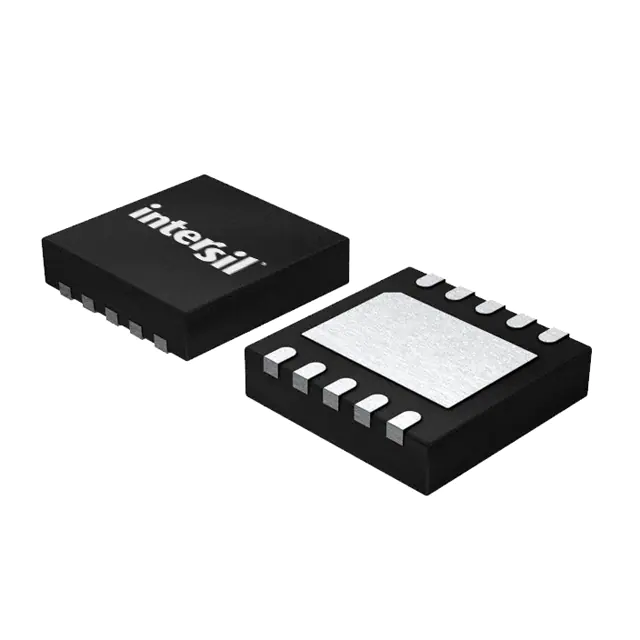
- Part No.:
- ISL6627IRZ
- Manufacturer:
- Renesas
- Category:
- Special Purpose Regulators
- Package:
- 10-VFDFN Exposed Pad
- Datasheet:
-
 ISL6627IRZ.pdf
- Description:
- IC REG CTRLR INTEL 1OUT 10DFN
- Quantity:
- Payment:

- Shipping:

Inventory:100
Please send an inquiry. Send us your inquiry, and we will respond immediately.
Product details
Overview
ISL6627IRZ from Intersil is a VR11.1/VR12-compatible dual N-channel MOSFET driver for synchronous buck converters, delivering 4A lower-side sink current, 2A upper/lower source/sink capability, adaptive shoot-through protection, and diode emulation for light-load DCM operation in microprocessor core voltage regulation.
For engineers reviewing the ISL6627IRZ datasheet, ISL6627IRZ pinout, ISL6627IRZ application, or ISL6627IRZ equivalent, this page provides verified technical context, exact pin functions, real-world timing parameters (e.g., 8ns UGATE rise time, 14ns LGATE turn-off delay), thermal design guidance for its 3×3 DFN package, and validated alternative options for VRM designs requiring -40°C to +85°C operation.
Technical Context
The ISL6627IRZ implements an advanced PWM protocol that detects PSI# commands from VR11.1/VR12 controllers to activate diode emulation-enabling discontinuous conduction mode by turning off LGATE at inductor zero-current crossing. Its adaptive shoot-through protection monitors UGATE-PHASE and LGATE voltages to dynamically adjust dead time, preventing simultaneous conduction while minimizing losses.
It supports fixed deadtime programming via the TD pin (7–40ns configurable delays), integrates a 36V bootstrap diode with overcharge prevention, and includes a 20kΩ internal high-side gate-to-source resistor to suppress dV/dt-induced self-turn-on. The driver operates from a 5V ±10% VCC supply and features POR thresholds of 3.20–4.40V rising and 3.00–4.00V falling.
Key Specifications
| Parameter | Value and Actual Design Meaning |
|---|---|
| VCC Supply | 5V ±10% - powers gate drivers and logic; requires low-ESR ceramic decoupling to GND. |
| Lower-Side Sink Current | 4A - enables fast discharge of large lower-MOSFET gates, critical for high-current VRMs. |
| UGATE Rise/Fall Time | 8ns (10–90%, 3nF load) - ensures rapid switching transitions to minimize overlap losses. |
| LGATE Turn-Off Propagation Delay | 14ns - defines minimum time between PWM falling edge and LGATE deactivation. |
| Operating Ambient Range | -40°C to +85°C - qualified for industrial and computing environments with extended thermal margins. |
| Bootstrap Voltage Rating | 36V (<200ns pulse) - withstands high-voltage transients during PHASE node ringing without overstress. |
| Diode Emulation Min. LGATE ON-Time | 330ns (typical) - guarantees sufficient conduction window for reliable zero-current detection in DCM. |
Pinout & Package
Dual Flat No-Lead (DFN) 10-lead 3×3 mm package with exposed thermal pad (EPAD) soldered to GND plane for enhanced heat dissipation; RoHS-compliant, MSL3 per J-STD-020.
| Pin/Terminal | Circuit Role | Design Meaning |
|---|---|---|
| 1 UGATE | Upper gate drive output | Drives gate of high-side N-MOSFET; referenced to PHASE node. |
| 2 BOOT | Floating bootstrap supply | Provides charge path for UGATE; connects to bootstrap capacitor between BOOT and PHASE. |
| 3 TD | Deadtime programming input | Resistor tie to GND/VCC selects fixed propagation delay; open = adaptive mode. |
| 4 PWM | Controller interface input | Accepts three-state PWM signal (0V/2.5V/5V) to decode VR11.1/VR12 protocols including PSI#. |
| 5 GND | Bias and power ground reference | Common return for all signals and driver power paths; must connect to EPAD. |
| 6 LGATE | Lower gate drive output | Drives gate of low-side N-MOSFET; referenced to GND. |
| 7 VCC | Driver bias supply | 5V input powering internal logic and gate drivers; requires local 1µF ceramic decoupling. |
| 8 NC | No connection | Unbonded pin; must remain unconnected on PCB. |
| 9 EN | Enable control input | Logic-high (>1.4V) enables driver; logic-low (<1.55V) disables outputs and reduces standby current to 1.15mA. |
| 10 PHASE | Switching node connection | Connects to source of upper MOSFET and drain of lower MOSFET; serves as return path for UGATE drive current. |
| EPAD | Thermal and electrical ground | Exposed copper pad under package; must be soldered directly to GND plane with ≥4 thermal vias for thermal management. |
Key Features
| Feature | Design Value |
|---|---|
| VR11.1/VR12 compatibility | Direct interoperability with Intersil's voltage regulator controllers using PSI# and three-state PWM signaling. |
| Adaptive shoot-through protection | Real-time monitoring of UGATE-PHASE and LGATE voltages eliminates need for manual deadtime tuning across FET variants. |
| Programmable fixed deadtime | TD pin resistor selection enables precise optimization of UGATE/LGATE timing margins for efficiency vs. robustness trade-offs. |
| Integrated 20kΩ high-side gate resistor | Prevents Miller-induced self-turn-on during high-dV/dt startup without external components or efficiency penalty. |
| Bootstrap capacitor overcharge prevention | Internal circuitry clamps negative PHASE excursions to avoid excessive BOOT voltage and upper-driver overstress. |
Applications
| Server CPU Core Regulator | AI Accelerator VRM |
|---|---|
Use Scenario: High-current, multi-phase buck converter supplying dynamic core voltage to Intel Xeon or AMD EPYC processors under rapid load transients. IC Role / Device Role / Timing Role: Dual gate driver controlling upper/lower N-MOSFETs per phase; executes diode emulation during PSI#-triggered light-load states to maintain >90% efficiency at 5A output. Use Value: Adaptive deadtime prevents shoot-through during GHz-scale frequency scaling; 4A LGATE sink sustains <10ns switching transitions at 1MHz+ frequencies. | Use Scenario: Compact, high-density VRM for NVIDIA GPU or custom AI ASIC requiring tight voltage accuracy and thermal headroom in 1U chassis. IC Role / Device Role / Timing Role: Synchronous rectified buck driver enabling DCM operation below 10% load; TD pin programmed for 15ns fixed UGATE→LGATE delay to balance efficiency and noise. Use Value: 3×3 DFN package with EPAD allows direct thermal coupling to heatsink; integrated bootstrap diode eliminates external Schottky, reducing BOM count by one component. |
| Industrial Edge Computing PSU | High-Frequency Notebook VRD |
Use Scenario: Fanless embedded system operating continuously at -40°C to +85°C ambient, powering ARM-based SoC with burst-mode workloads. IC Role / Device Role / Timing Role: Enables stable CCM-to-DCM transition via PSI# detection; EN pin used for system-level power sequencing with 1.4V enable threshold. Use Value: -40°C to +85°C rating matches industrial temperature envelope; POR hysteresis (300mV typ.) ensures clean startup across wide input voltage range. | Use Scenario: Thin-and-light laptop motherboard where board space and thermal profile constrain VRM layout. IC Role / Device Role / Timing Role: Gate driver in single-phase core regulator; uses 8ns UGATE rise/fall times and 14ns LGATE turn-off delay to support >1.5MHz switching without compromising EMI. Use Value: Near chip-scale 3×3 DFN footprint saves >30% PCB area vs. SOIC-8; EPAD vias reduce junction-to-ambient θJA to 51°C/W for passive cooling. |
Equivalent & Alternatives
The following parts are listed as comparable options for similar synchronous buck MOSFET driver applications.
| Alternative Part | Technical Difference | Application Difference | Selection Advice |
|---|---|---|---|
| ISL6622CRZ | Same family, but rated for 0°C to +70°C ambient; lacks PSI# protocol support and diode emulation. | Suitable only for commercial-temperature desktop VRMs without light-load efficiency requirements. | Select ISL6622CRZ only if ambient stays within 0–70°C and VR11.1/VR12 compatibility is unnecessary. |
| MP86957DQKT-LF-Z | Monolithic 2-phase controller with integrated drivers; no separate TD pin or adaptive shoot-through; max 1.2MHz switching. | Reduces component count but sacrifices timing flexibility and VR11.1 protocol fidelity. | Choose MP86957 when board space is critical and fixed-frequency, non-PSI# operation suffices. |
Compared with ISL6627IRZ, ISL6622CRZ offers lower temperature grade and no diode emulation, limiting light-load efficiency; MP86957DQKT-LF-Z integrates control logic but removes programmable deadtime and adaptive protection-making ISL6627IRZ the sole option for VR11.1/VR12-compliant, thermally rugged, high-efficiency core regulation.
Availability
ISL6627IRZ is available at Aetrix Electronics and suitable for server CPU core regulators, AI accelerator VRMs, and industrial edge computing PSUs requiring stable component supply across extended temperature ranges and long production lifecycles.
Supply support for ISL6627IRZ includes scheduled delivery planning, volume procurement assistance, BOM continuity management, traceable sourcing, and lifecycle availability coordination for OEM customers, industrial embedded developers, connected-device designers, and electronics production programs.
Manufacturer
Intersil Corporation designs high-performance analog, mixed-signal, and power management semiconductors for industrial, computing, and consumer markets, operating under Renesas Electronics since 2017.
The ISL6627IRZ belongs to Intersil's VRM driver product line, engineered specifically for high-efficiency, high-frequency core voltage regulation in advanced microprocessors compliant with VR11.1 and VR12 specifications.
FAQ
What is the maximum allowable ambient temperature for continuous operation of the ISL6627IRZ?
The ISL6627IRZ is specified for continuous operation from -40°C to +85°C ambient temperature. Its maximum junction temperature is +125°C, and thermal resistance θJA is 51°C/W in the 3×3 DFN package. Proper PCB layout-including EPAD soldering to GND with ≥4 thermal vias-is required to maintain safe junction temperatures at full load across this range. Derating applies above +85°C ambient.
How does the ISL6627IRZ implement diode emulation, and what triggers it?
The ISL6627IRZ activates diode emulation upon detecting a PSI# (Power State Indicator) command from a compatible VR11.1 or VR12 controller via the PWM pin. During PSI#, it monitors inductor current zero-crossing and turns off LGATE to force discontinuous conduction mode (DCM), preventing reverse current flow. Minimum LGATE ON-time is 330ns (typical) to ensure reliable detection. This occurs only when PSI# is asserted-not in standard CCM operation.
Can the ISL6627IRZ drive both high-side and low-side N-channel MOSFETs in a single-phase buck converter?
Yes, the ISL6627IRZ is explicitly designed as a dual N-channel MOSFET driver for synchronous rectified buck topologies. UGATE drives the high-side N-MOSFET gate referenced to the PHASE node, while LGATE drives the low-side N-MOSFET gate referenced to GND. It includes integrated bootstrap circuitry (36V-rated internal Schottky diode) and adaptive shoot-through protection to coordinate switching safely and efficiently.
What is the function of the TD pin on the ISL6627IRZ, and how does it affect performance?
TD (Deadtime) pin on the ISL6627IRZ selects between adaptive and fixed propagation delay modes. When left floating, it enables adaptive shoot-through protection that dynamically adjusts deadtime based on gate voltage transitions. When tied to GND or VCC via resistor (e.g., 360kΩ to GND), it configures fixed delays-such as 17ns LGATE-fall-to-UGATE-rise-to optimize efficiency in stable, known-FET applications. Tolerance is ±30%; worst-case margining is required.
Does the ISL6627IRZ include built-in protection against high dV/dt at the PHASE node?
Yes, the ISL6627IRZ incorporates two key protections against high dV/dt: (1) a 20kΩ integrated high-side gate-to-source resistor that suppresses Miller-induced self-turn-on of the upper MOSFET during fast PHASE node transitions, and (2) bootstrap capacitor overcharge prevention that clamps negative PHASE excursions to limit BOOT voltage stress. These features eliminate the need for external gate resistors or snubbers in most designs.
ISL6627IRZ Specifications
- Product attributes
- Attribute value
- Manufacturer:
- Renesas
- Series:
- -
- Package/Case:
- 10-VFDFN Exposed Pad
- Packaging:
- Tube
- Product Status:
- Obsolete
- Applications:
- Controller, Intel VR11.1, VR12
- Voltage - Input:
- 4.5V ~ 5.5V
- Number of Outputs:
- 1
- Voltage - Output:
- -
- Operating Temperature:
- -40°C ~ 85°C
- Grade:
- -
- Qualification:
- -
- Mounting Type:
- Surface Mount
- Supplier Device Package:
- 10-DFN (3x3)
ISL6627IRZ FAQ
1.How can I place an order for ISL6627IRZ through Aetrix?
Please submit a Request for Quotation (RFQ) for ISL6627IRZ on Aetrix. Our sales agent will provide a competitive quotation and guide you through the order confirmation once you accept the terms.
2.Are the price and stock information for ISL6627IRZ reliable?
The price and inventory of ISL6627IRZ are updated periodically and may fluctuate due to market conditions. Stock and pricing data are typically refreshed every 24 hours. Quotation validity for ISL6627IRZ is usually 5 days.
3.What payment methods are accepted for ISL6627IRZ?
We accept Wire Transfer, PayPal, Credit Card, Western Union, MoneyGram, and Escrow for ISL6627IRZ transactions.
Note: Certain payment methods may incur a processing fee.
4.How is shipping managed for ISL6627IRZ?
ISL6627IRZ orders can be shipped via leading logistics carriers, including DHL, UPS, FedEx, TNT, or Registered Mail.
Once your ISL6627IRZ order is processed, you will receive an email with the shipment details and tracking number.
Note: Tracking information may take up to 24 hours to appear. Express delivery typically takes 3–5 business days.
5.How can I obtain technical support or documentation for ISL6627IRZ?
For technical support, including ISL6627IRZ datasheets, pinout diagrams, or application guidance, please contact our engineering support team. They can provide detailed documentation and assistance for your ISL6627IRZ requirements.
6.How does Aetrix verify that ISL6627IRZ is sourced from the original manufacturer or authorized distributors?
All ISL6627IRZ products on Aetrix are procured from qualified distributors and authorized channels. Our dedicated quality assurance team conducts strict verification, including traceability checks and, if necessary, third-party testing. This ensures that ISL6627IRZ meets industry standards.
7.What is the process for return or replacement of ISL6627IRZ?
All ISL6627IRZ units undergo pre-shipment inspection (PSI). If there is an issue with ISL6627IRZ, returns or replacements are accepted under the following conditions:
1.Quantity discrepancies, incorrect items, or visible external defects (such as breakage or corrosion), acknowledged by Aetrix.
2.The issue is reported within 90 days of delivery.
3.The ISL6627IRZ part is unused and in its original packaging.
Return procedure for ISL6627IRZ:
1.Submit a request within 90 days.
2.Obtain a Return Material Authorization (RMA) from Aetrix.
ISL6627IRZ Tags

-
TPS51206DSQR
Texas Instruments

-
TPS51200DRCR
Texas Instruments
-
TPS51200DRCT
Texas Instruments

-
TPS62740DSSR
Texas Instruments

-
TPS51100DGQR
Texas Instruments

-
NCP51200MNTXG
onsemi
-
NCP51400MNTXG
onsemi

-
RT9026GSP
Richtek USA Inc.

-
LP2998MRX/NOPB
Texas Instruments
-
TPS51200QDRCRQ1
Texas Instruments

-
DPA423GN-TL
Power Integrations
-
LM10011SD/NOPB
Texas Instruments
Tech Hub

TTL and CMOS logic families differ in thresholds, loading, output drive, power and timing. This engineering guide compares 74HC and 74HCT, calculates noise margins and checks 3.3 V/5 V compatibility.

A practical engineering guide to 3.3V and 5V logic compatibility, input thresholds, resistor dividers, translator ICs, MOSFET level shifting, I2C pull-ups, timing limits and power-sequencing risks.

The 74HC595 uses push-pull logic outputs, while the TPIC6B595 uses 50 V open-drain DMOS sinks for higher-power loads. This guide compares timing, current limits, 3.3 V interfacing, load wiring, thermal…

The 74HC595 converts serial data into eight stable parallel outputs. This guide covers pin functions, shift and storage timing, OE and MR behavior, drive-current limits, cascading, voltage compatibilit…

A technical comparison of level-sensitive latches and edge-triggered flip-flops, covering timing windows, setup and hold limits, master–slave operation, time borrowing, race-through, HDL inference and…

A D latch stores one bit while Enable controls when data can pass. This reference covers gate-level operation, truth tables, transparency, setup and hold timing, LE versus OE, common ICs and practical …

An SR latch stores one bit through cross-coupled feedback. This engineering reference covers NOR and NAND implementations, truth tables, forbidden-state recovery, gated operation, switch debouncing, fa…

Latch circuits retain one bit through feedback. This technical reference covers SR and D latches, truth tables, transparency, timing limits, latch-versus-flip-flop behavior, applications and common log…

An engineering guide to LED driver operation, constant-current and constant-voltage outputs, linear and switching topologies, dimming, IC selection, calculations, replacement compatibility, and fault c…

Operational amplifier guide covering op amp basics, feedback, ideal vs real op amps, common configurations, buffer circuits, offset, bias current, gain-bandwidth, slew rate, rail-to-rail limits and sel…


