
 My Inquiry
 My Account


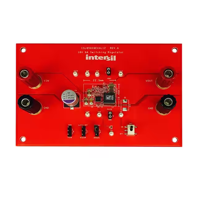
Renesas ISL85009EVAL1Z
- Part No.:
- ISL85009EVAL1Z
- Manufacturer:
- Renesas
- Package:
- Datasheet:
-
 ISL85009EVAL1Z.pdf
- Description:
- EVAL BOARD FOR ISL85009
- Quantity:
- Payment:

- Shipping:

Inventory:1,816
Please send an inquiry. Send us your inquiry, and we will respond immediately.
Product details
Overview
ISL85009EVAL1Z from Intersil is an evaluation board designed to rapidly assess the ISL85009 9A synchronous buck regulator, configured for 1.8V/9A output with 4.5V–18V input range, 600kHz default switching frequency, and -40°C to +85°C operating temperature. It supports mode selection (DEM/FCCM), OCP configuration (Hiccup/Latch-Off), and external clock synchronization.
For engineers reviewing the ISL85009EVAL1Z datasheet, ISL85009EVAL1Z pinout, ISL85009EVAL1Z application, or ISL85009EVAL1Z equivalent, this board enables fast validation of high-current DC/DC conversion in battery-powered and industrial power systems - especially where programmable soft-start, power-good signaling, and thermal-aware layout are critical.
Technical Context
The ISL85009EVAL1Z implements the ISL85009 IC in a fully assembled, tested, and optimized layout - featuring integrated bootstrap diode, internal compensation, and configurable EN control via SW5. It exposes all key regulator signals (PVIN, VOUT, PHASE, BOOT, FB, COMP, PG, SYNC) through test points and connectors.
Board-level features include jumper-selectable frequency (300kHz/600kHz), operating mode (Diode Emulation/Forced CCM), and overcurrent protection (Hiccup/Latch-Off), plus dedicated connectors for input (J1/J3), output (J2/J4), and probing (J6/J7, VOUT/GND, SYNC, EN, PG).
Key Specifications
| Parameter | Value and Actual Design Meaning |
|---|---|
| Input Voltage Range | 4.5V to 18V - supports multi-cell Li-ion batteries and standard 5V/12V rails without external pre-regulation. |
| Output Voltage | 1.8V nominal - factory-configured via R1/R2 feedback divider; adjustable using Equation 1 per UG112. |
| Max Output Current | 9A continuous - validated with thermal vias, multilayer PCB, and low-ESR output capacitors (C10–C12). |
| Switching Frequency | Default 600kHz - selectable to 300kHz via J10; enables trade-off between efficiency and EMI/noise performance. |
| Soft-Start Time | 3ms internally set - limits inrush current during startup; prevents input rail droop in sensitive systems. |
| Operating Temperature | -40°C to +85°C - rated for industrial and embedded environments; validated with thermal imaging per typical curves. |
| Power-Good Signal | Active-high PG pin - provides system-level sequencing and fault indication with ±5% output voltage tolerance window. |
Availability
ISL85009EVAL1Z is available at Aetrix Electronics and suitable for industrial power design, battery management systems, and FPGA/ASIC core voltage evaluation requiring stable component supply, rapid prototyping support, and documented thermal and EMI performance.
Supply support for ISL85009EVAL1Z includes scheduled delivery planning, volume procurement assistance, BOM continuity management, traceable sourcing, and lifecycle availability coordination for OEM customers, industrial embedded developers, connected-device designers, and electronics production programs.
Manufacturer
Intersil Corporation (now part of Renesas Electronics) is a semiconductor company specializing in precision analog, power management, and interface ICs for industrial, computing, and communications applications.
The ISL85009EVAL1Z belongs to Intersil's high-current DC/DC evaluation platform family, developed to accelerate adoption of their synchronous buck regulators in demanding power-constrained designs.
FAQ
What is the primary function of the ISL85009EVAL1Z?
The ISL85009EVAL1Z is an evaluation board for the ISL85009 9A synchronous buck regulator. Its primary function is to enable rapid hardware validation of the IC's performance - including regulation accuracy, transient response, thermal behavior, and configurability - under real-world conditions like 4.5V–18V input and 1.8V/9A output. The ISL85009EVAL1Z includes all necessary passives, jumpers, and test points to eliminate prototype development time.
Can the output voltage of the ISL85009EVAL1Z be adjusted?
Yes, the ISL85009EVAL1Z supports output voltage adjustment via the external resistor divider formed by R1 and R2 on the feedback (FB) pin. Though factory-configured for 1.8V, Equation 1 in UG112 allows recalculation of R2 based on R1 and desired VOUT. The ISL85009EVAL1Z schematic and bill of materials confirm R1 (200kΩ) and R2 (100kΩ) placement, enabling straightforward reconfiguration for other voltages within the ISL85009's 0.6V–VIN range.
How do I configure the ISL85009EVAL1Z for Forced CCM operation?
To configure the ISL85009EVAL1Z for Forced Continuous Conduction Mode (FCCM), install jumper J9 in the FCCM position as specified in UG112 Section "Selection Switch and Jumper Descriptions". This overrides light-load diode emulation and maintains constant switching frequency across all load conditions - essential for noise-sensitive applications or when consistent EMI signature is required. The ISL85009EVAL1Z user guide confirms FCCM selection directly controls the MODE pin behavior of the underlying ISL85009 IC.
Does the ISL85009EVAL1Z support external clock synchronization?
Yes, the ISL85009EVAL1Z supports external clock synchronization via the SYNC test point. Applying a clean TTL- or CMOS-compatible clock signal (100kHz–1MHz) to SYNC synchronizes the ISL85009's internal oscillator, eliminating beat frequencies in multi-rail systems. UG112 explicitly states this capability and references the ISL85009 datasheet for pulse width and voltage level requirements - confirming full functional support on the ISL85009EVAL1Z board.
What thermal design elements are implemented on the ISL85009EVAL1Z?
The ISL85009EVAL1Z incorporates multiple thermal design elements: a four-layer PCB stack-up, thermal vias under the ISL85009FRZ TDFN package (U1), wide copper pours for PVIN/VOUT/GND planes, and strategic placement of bulk (C10–C12) and ceramic (C9/C13/C14) output capacitors near the IC. UG112 Section "PCB Layout Considerations" mandates these practices, and thermal performance is validated in Figure 8–11, showing stable 1.8V regulation at 9A and 12V input across -40°C to +85°C.
ISL85009EVAL1Z Specifications
- Product attributes
- Attribute value
- Manufacturer:
- Renesas
- Series:
- -
- Packaging:
- Bulk
- Product Status:
- Active
- Main Purpose:
- DC/DC, Step Down
- Outputs and Type:
- 1 Non-Isolated Output
- Voltage - Output:
- -
- Current - Output:
- 1.8V
- Voltage - Input:
- 9A
- Regulator Topology:
- 4.5V ~ 18V
- Frequency - Switching:
- Buck
- Contents:
- 600kHz
- Utilized IC / Part:
- Board(s)
- Power - Output:
- ISL85009
ISL85009EVAL1Z FAQ
1.How can I place an order for ISL85009EVAL1Z through Aetrix?
Please submit a Request for Quotation (RFQ) for ISL85009EVAL1Z on Aetrix. Our sales agent will provide a competitive quotation and guide you through the order confirmation once you accept the terms.
2.Are the price and stock information for ISL85009EVAL1Z reliable?
The price and inventory of ISL85009EVAL1Z are updated periodically and may fluctuate due to market conditions. Stock and pricing data are typically refreshed every 24 hours. Quotation validity for ISL85009EVAL1Z is usually 5 days.
3.What payment methods are accepted for ISL85009EVAL1Z?
We accept Wire Transfer, PayPal, Credit Card, Western Union, MoneyGram, and Escrow for ISL85009EVAL1Z transactions.
Note: Certain payment methods may incur a processing fee.
4.How is shipping managed for ISL85009EVAL1Z?
ISL85009EVAL1Z orders can be shipped via leading logistics carriers, including DHL, UPS, FedEx, TNT, or Registered Mail.
Once your ISL85009EVAL1Z order is processed, you will receive an email with the shipment details and tracking number.
Note: Tracking information may take up to 24 hours to appear. Express delivery typically takes 3–5 business days.
5.How can I obtain technical support or documentation for ISL85009EVAL1Z?
For technical support, including ISL85009EVAL1Z datasheets, pinout diagrams, or application guidance, please contact our engineering support team. They can provide detailed documentation and assistance for your ISL85009EVAL1Z requirements.
6.How does Aetrix verify that ISL85009EVAL1Z is sourced from the original manufacturer or authorized distributors?
All ISL85009EVAL1Z products on Aetrix are procured from qualified distributors and authorized channels. Our dedicated quality assurance team conducts strict verification, including traceability checks and, if necessary, third-party testing. This ensures that ISL85009EVAL1Z meets industry standards.
7.What is the process for return or replacement of ISL85009EVAL1Z?
All ISL85009EVAL1Z units undergo pre-shipment inspection (PSI). If there is an issue with ISL85009EVAL1Z, returns or replacements are accepted under the following conditions:
1.Quantity discrepancies, incorrect items, or visible external defects (such as breakage or corrosion), acknowledged by Aetrix.
2.The issue is reported within 90 days of delivery.
3.The ISL85009EVAL1Z part is unused and in its original packaging.
Return procedure for ISL85009EVAL1Z:
1.Submit a request within 90 days.
2.Obtain a Return Material Authorization (RMA) from Aetrix.
ISL85009EVAL1Z Tags
-
DFR0571
DFRobot
-
DFR0379
DFRobot
-
DFR0205
DFRobot
-
1385
Adafruit Industries LLC
-
COM-15208
SparkFun Electronics
-
1944
Adafruit Industries LLC
-
2465
Adafruit Industries LLC
-
DC2468A
Analog Devices Inc.
-
DC2841A
Analog Devices Inc.

-
TPS552892EVM-111
Texas Instruments
-
TPS55289EVM-093
Texas Instruments
-
EPC9158
EPC
Tech Hub

TTL and CMOS logic families differ in thresholds, loading, output drive, power and timing. This engineering guide compares 74HC and 74HCT, calculates noise margins and checks 3.3 V/5 V compatibility.

A practical engineering guide to 3.3V and 5V logic compatibility, input thresholds, resistor dividers, translator ICs, MOSFET level shifting, I2C pull-ups, timing limits and power-sequencing risks.

The 74HC595 uses push-pull logic outputs, while the TPIC6B595 uses 50 V open-drain DMOS sinks for higher-power loads. This guide compares timing, current limits, 3.3 V interfacing, load wiring, thermal…

The 74HC595 converts serial data into eight stable parallel outputs. This guide covers pin functions, shift and storage timing, OE and MR behavior, drive-current limits, cascading, voltage compatibilit…

A technical comparison of level-sensitive latches and edge-triggered flip-flops, covering timing windows, setup and hold limits, master–slave operation, time borrowing, race-through, HDL inference and…

A D latch stores one bit while Enable controls when data can pass. This reference covers gate-level operation, truth tables, transparency, setup and hold timing, LE versus OE, common ICs and practical …

An SR latch stores one bit through cross-coupled feedback. This engineering reference covers NOR and NAND implementations, truth tables, forbidden-state recovery, gated operation, switch debouncing, fa…

Latch circuits retain one bit through feedback. This technical reference covers SR and D latches, truth tables, transparency, timing limits, latch-versus-flip-flop behavior, applications and common log…

An engineering guide to LED driver operation, constant-current and constant-voltage outputs, linear and switching topologies, dimming, IC selection, calculations, replacement compatibility, and fault c…

Operational amplifier guide covering op amp basics, feedback, ideal vs real op amps, common configurations, buffer circuits, offset, bias current, gain-bandwidth, slew rate, rail-to-rail limits and sel…


