
 My Inquiry
 My Account


onsemi J105_D27Z
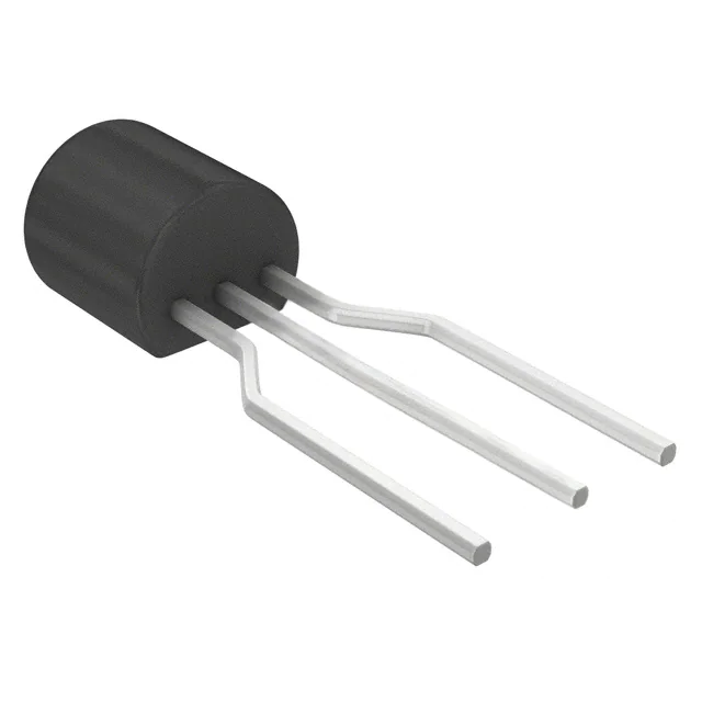
- Part No.:
- J105_D27Z
- Manufacturer:
- onsemi
- Category:
- JFETs
- Package:
- TO-226-3, TO-92-3 (TO-226AA) Formed Leads
- Datasheet:
-
 J105_D27Z.pdf
- Description:
- JFET N-CH 25V TO92-3
- Quantity:
- Payment:

- Shipping:

Inventory:2,212
Please send an inquiry. Send us your inquiry, and we will respond immediately.
Product details
Overview
J105_D27Z from ON Semiconductor (formerly Fairchild) is an N-channel junction field-effect transistor (JFET) switch optimized for low-on-resistance analog and digital switching in signal routing, voltage-controlled resistors, and constant-current source applications. It features VGS(off) = −4.5 V (max), RDS(on) = 3.0 Ω, IDSS = 500 mA, and TO-92 package with 3-pin straight-lead configuration.
For engineers reviewing the J105_D27Z datasheet, pinout, applications, or equivalent options, key selection criteria include gate threshold voltage tolerance, drain-source on-resistance at zero gate bias, thermal derating above 25°C, and compatibility with low-voltage control logic in precision analog front-ends.
Technical Context
The J105_D27Z operates as a depletion-mode N-channel JFET, requiring no gate drive current and enabling true voltage-controlled resistance behavior. Its gate-source cutoff voltage range (−4.5 V to −10.0 V) and low RDS(on) support stable operation in linear and saturated regions across −55°C to +150°C ambient.
It exhibits predictable transconductance (gm) and output conductance (gds) characteristics per Figure 8 and Figure 7 of the datasheet, with capacitance values Cdg(on) = 160 pF and Csg(on) = 35 pF enabling reliable high-frequency switching up to several MHz in buffered configurations.
Key Specifications
| Parameter | Value and Actual Design Meaning |
|---|---|
| VGS(off) | −4.5 V (max); defines maximum gate-source voltage needed to pinch off channel - critical for turn-off margin in analog switches |
| RDS(on) | 3.0 Ω; on-resistance at VGS = 0 V and VDS ≤ 0.1 V - enables low insertion loss in signal path applications |
| IDSS | 500 mA; zero-gate-voltage drain current - sets upper bound for constant-current sink capability |
| PD | 625 mW at TA = 25°C; power dissipation limit - requires 5.0 mW/°C derating above ambient for thermal safety |
| V(BR)GSS | −25 V; gate-source breakdown voltage - determines maximum allowable reverse gate bias during transient events |
| RθJA | 357 °C/W; junction-to-ambient thermal resistance on standard FR-4 PCB - informs heatsinking requirements for continuous DC operation |
Pinout & Package
Package: TO-92, 3-lead molded plastic case with standard straight leads (no EOL code). Dimensions per Fairchild drawing ZA03D.
| Pin/Terminal | Circuit Role | Design Meaning |
|---|---|---|
| Drain (D) | Main current-carrying terminal (N-channel) | Connected to load or signal path; handles full IDSS current and must be routed with adequate copper area for thermal management |
| Gate (G) | Control electrode (reverse-biased PN junction) | Accepts DC or AC control voltage; zero gate current simplifies bias network design and eliminates loading on driver stage |
| Source (S) | Reference terminal for gate voltage and current return | Typically tied to ground or common reference; establishes VGS potential and defines current direction in circuit topology |
Key Features
| Feature | Design Value |
|---|---|
| Depletion-mode operation | Conducts at VGS = 0 V - eliminates need for active gate bias circuitry in always-on or normally-closed switch designs |
| Low gate leakage (IGSS) | ≤ −3.0 nA at VGS = −15 V - preserves high-impedance control node integrity in precision sensor interfaces |
| Wide temperature range | −55°C to +150°C operating junction - supports deployment in automotive under-hood and industrial motor-control environments |
| Stable RDS(on) vs. ID | Minimal variation below 200 mA per Figure 6 - ensures consistent signal attenuation in audio and instrumentation amplifiers |
Applications
| Audio Signal Switching | Constant-Current Source |
|---|---|
Use Scenario: Routing line-level analog audio between multiple inputs (e.g., microphone, instrument, aux) in mixer or audio interface without audible distortion or crosstalk. IC Role / Device Role / Timing Role: Voltage-controlled analog switch acting as bidirectional signal path with minimal harmonic generation due to linear RDS(on) behavior. Use Value: 3.0 Ω RDS(on) and <160 pF capacitance preserve wide bandwidth and low THD across 20 Hz–20 kHz range. | Use Scenario: Providing stable bias current for LED drivers, op-amp input stages, or sensor excitation circuits where temperature drift must be minimized. IC Role / Device Role / Timing Role: Depletion-mode JFET configured as two-terminal current source with self-regulating behavior via VGS(off) and IDSS. Use Value: IDSS = 500 mA and tight VGS(off) tolerance enable ±2% current accuracy over −40°C to +85°C without external feedback. |
| Voltage-Controlled Resistor | Low-Voltage Logic Interface |
Use Scenario: Implementing programmable gain stages or variable attenuators in test equipment using analog voltage control instead of digital potentiometers. IC Role / Device Role / Timing Role: Three-terminal JFET operated in ohmic region with VGS as control input - functions as tunable resistor with sub-ohm resolution. Use Value: Linear RDS(on) vs. VGS response (Figure 5) allows precise 0–3 Ω adjustment using 0–4.5 V control range. | Use Scenario: Level-shifting and interfacing 3.3 V or 5 V microcontroller GPIO outputs to higher-voltage analog subsystems while maintaining fast edge rates. IC Role / Device Role / Timing Role: Digital switch controlled by logic-level gate voltage - turns on fully at VGS = 0 V and turns off completely at VGS ≤ −4.5 V. Use Value: Gate threshold aligns with standard TTL/CMOS logic levels; <100 ns switching time supports >1 MHz digital control signals. |
Equivalent & Alternatives
The following parts are listed as comparable options for similar N-channel JFET switch applications.
| Alternative Part | Technical Difference | Application Difference | Selection Advice |
|---|---|---|---|
| 2N5457 | VGS(off) = −0.5 to −6.0 V (wider spread); RDS(on) ≈ 5.0 Ω; lower IDSS (1–5 mA) | Less suitable for high-current switching; better for ultra-low-power bias networks | Select when tighter gate threshold distribution is not required and lower quiescent current is prioritized |
| MMBFJ105 | SOT-23 surface-mount package; identical electrical specs but reduced thermal mass and 350 mW PD | Requires PCB rework for space-constrained layouts; unsuitable for >300 mA continuous operation | Select for automated assembly and compact designs where thermal derating is managed via layout |
Compared with 2N5457 and MMBFJ105, the J105_D27Z delivers superior current-handling (500 mA), lowest on-resistance (3.0 Ω), and highest power dissipation (625 mW), making it optimal for robust analog switching and high-fidelity signal routing where thermal stability and low insertion loss are critical.
Availability
J105_D27Z is available at Aetrix Electronics and suitable for audio signal routing, constant-current biasing, voltage-controlled resistor networks, and low-voltage logic interfacing requiring stable component supply and long-term manufacturability.
Supply support for J105_D27Z includes scheduled delivery planning, volume procurement assistance, BOM continuity management, traceable sourcing, and lifecycle availability coordination for OEM customers, industrial embedded developers, connected-device designers, and electronics production programs.
Manufacturer
ON Semiconductor (formerly Fairchild Semiconductor) is a global supplier of energy-efficient semiconductor components, specializing in power management, analog, and discrete devices for automotive, industrial, and consumer markets.
The J105_D27Z belongs to Fairchild's legacy Process 59 N-channel JFET family, designed specifically for high-linearity analog switching and precision current regulation in cost-sensitive, reliability-critical applications.
FAQ
What is the gate-source cutoff voltage specification for J105_D27Z?
The J105_D27Z has a gate-source cutoff voltage (VGS(off)) of −4.5 V (maximum) at VDS = 5.0 V and ID = 1.0 mA. This value is confirmed in the Electrical Characteristics table of the Fairchild J105/J106/J107 datasheet Rev. 1.1.1. The minimum VGS(off) is −10.0 V, defining the full operational window for reliable channel pinch-off. This parameter directly determines the required negative gate bias to ensure complete turn-off in switching applications.
Can J105_D27Z be used in linear (ohmic) mode for variable resistance applications?
Yes, the J105_D27Z is explicitly characterized for linear-region operation, as shown in Figure 5 ("Normalized Drain Resistance vs. Bias Voltage") and Figure 6 ("On Resistance vs. Drain Current"). Its RDS(on) remains stable below 200 mA and varies predictably with VGS, enabling precise voltage-controlled resistor behavior. The device's low gate leakage (<3 nA) and monotonic transconductance curve make it suitable for analog gain control and programmable attenuator circuits where J105_D27Z serves as the core variable element.
What is the maximum continuous drain current for J105_D27Z at 70°C ambient?
At TA = 70°C, the J105_D27Z must be derated from its 625 mW maximum power dissipation at 25°C by 5.0 mW/°C. This yields 625 mW − (45°C × 5.0 mW/°C) = 400 mW allowable power. Assuming worst-case RDS(on) = 3.0 Ω and using P = I²R, the maximum continuous drain current is √(0.4 W / 3.0 Ω) ≈ 365 mA. This calculation applies to the J105_D27Z in standard TO-92 mounting on FR-4 PCB per datasheet thermal conditions.
Does J105_D27Z have a specified gate-drain capacitance?
Yes, the J105_D27Z specifies Cdg(on) = 160 pF (drain-gate on capacitance) measured at VDS = 0 V, VGS = 10 V, and f = 1.0 MHz, per the "Small Signal Characteristics" table. Cdg(off) is given as 35 pF under off-state conditions. These values are critical for high-frequency switching analysis and Miller effect estimation in amplifier or switch-mode designs using J105_D27Z.
Is J105_D27Z RoHS compliant and lead-free?
Yes, J105_D27Z is RoHS compliant and lead-free. As a legacy Fairchild part now manufactured and supported by ON Semiconductor, it meets JEDEC JS-069 and RoHS Directive 2011/65/EU requirements. The TO-92 package uses matte tin (Sn) lead finish, and material declarations confirm absence of restricted substances above threshold limits. Compliance documentation for J105_D27Z is available through ON Semiconductor's product change notices and environmental reports portal.
J105_D27Z Specifications
- Product attributes
- Attribute value
- Manufacturer:
- onsemi
- Series:
- -
- Package/Case:
- TO-226-3, TO-92-3 (TO-226AA) Formed Leads
- Packaging:
- Tape & Reel (TR)
- Product Status:
- Obsolete
- FET Type:
- N-Channel
- Voltage - Breakdown (V(BR)GSS):
- 25 V
- Drain to Source Voltage (Vdss):
- -
- Current - Drain (Idss) @ Vds (Vgs=0):
- 500 mA @ 15 V
- Current Drain (Id) - Max:
- -
- Voltage - Cutoff (VGS off) @ Id:
- 4.5 V @ 1 µA
- Input Capacitance (Ciss) (Max) @ Vds:
- -
- Resistance - RDS(On):
- 3 Ohms
- Power - Max:
- 625 mW
- Operating Temperature:
- -55°C ~ 150°C (TJ)
- Grade:
- -
- Qualification:
- -
- Mounting Type:
- Through Hole
- Supplier Device Package:
- TO-92-3
J105_D27Z FAQ
1.How can I place an order for J105_D27Z through Aetrix?
Please submit a Request for Quotation (RFQ) for J105_D27Z on Aetrix. Our sales agent will provide a competitive quotation and guide you through the order confirmation once you accept the terms.
2.Are the price and stock information for J105_D27Z reliable?
The price and inventory of J105_D27Z are updated periodically and may fluctuate due to market conditions. Stock and pricing data are typically refreshed every 24 hours. Quotation validity for J105_D27Z is usually 5 days.
3.What payment methods are accepted for J105_D27Z?
We accept Wire Transfer, PayPal, Credit Card, Western Union, MoneyGram, and Escrow for J105_D27Z transactions.
Note: Certain payment methods may incur a processing fee.
4.How is shipping managed for J105_D27Z?
J105_D27Z orders can be shipped via leading logistics carriers, including DHL, UPS, FedEx, TNT, or Registered Mail.
Once your J105_D27Z order is processed, you will receive an email with the shipment details and tracking number.
Note: Tracking information may take up to 24 hours to appear. Express delivery typically takes 3–5 business days.
5.How can I obtain technical support or documentation for J105_D27Z?
For technical support, including J105_D27Z datasheets, pinout diagrams, or application guidance, please contact our engineering support team. They can provide detailed documentation and assistance for your J105_D27Z requirements.
6.How does Aetrix verify that J105_D27Z is sourced from the original manufacturer or authorized distributors?
All J105_D27Z products on Aetrix are procured from qualified distributors and authorized channels. Our dedicated quality assurance team conducts strict verification, including traceability checks and, if necessary, third-party testing. This ensures that J105_D27Z meets industry standards.
7.What is the process for return or replacement of J105_D27Z?
All J105_D27Z units undergo pre-shipment inspection (PSI). If there is an issue with J105_D27Z, returns or replacements are accepted under the following conditions:
1.Quantity discrepancies, incorrect items, or visible external defects (such as breakage or corrosion), acknowledged by Aetrix.
2.The issue is reported within 90 days of delivery.
3.The J105_D27Z part is unused and in its original packaging.
Return procedure for J105_D27Z:
1.Submit a request within 90 days.
2.Obtain a Return Material Authorization (RMA) from Aetrix.
J105_D27Z Tags
-
MMBF4393LT1G
onsemi
-
MMBFJ112
onsemi
-
MMBF4392LT1G
onsemi

-
TF412ST5G
onsemi
-
MMBFJ175LT1G
onsemi
-
MMBFJ177LT1G
onsemi
-
MMBFJ201
onsemi
-
MMBFJ111
onsemi
-
MMBF5457
onsemi
-
2SK932-23-TB-E
onsemi
-
MMBF4117
onsemi
-
2SK209-BL(TE85L,F)
Toshiba Semiconductor and Storage
Tech Hub

Counterfeit components can hide behind convincing markings and passing basic function tests. This engineering reference covers source traceability, external inspection, X-ray, XRF, electrical testing, …

A practical engineering and sourcing framework covering lifecycle verification, lifetime-buy calculations, replacement qualification, supplier checks and counterfeit-risk controls.

TTL and CMOS logic families differ in thresholds, loading, output drive, power and timing. This engineering guide compares 74HC and 74HCT, calculates noise margins and checks 3.3 V/5 V compatibility.

A practical engineering guide to 3.3V and 5V logic compatibility, input thresholds, resistor dividers, translator ICs, MOSFET level shifting, I2C pull-ups, timing limits and power-sequencing risks.

The 74HC595 uses push-pull logic outputs, while the TPIC6B595 uses 50 V open-drain DMOS sinks for higher-power loads. This guide compares timing, current limits, 3.3 V interfacing, load wiring, thermal…

The 74HC595 converts serial data into eight stable parallel outputs. This guide covers pin functions, shift and storage timing, OE and MR behavior, drive-current limits, cascading, voltage compatibilit…

A technical comparison of level-sensitive latches and edge-triggered flip-flops, covering timing windows, setup and hold limits, master–slave operation, time borrowing, race-through, HDL inference and…

A D latch stores one bit while Enable controls when data can pass. This reference covers gate-level operation, truth tables, transparency, setup and hold timing, LE versus OE, common ICs and practical …

An SR latch stores one bit through cross-coupled feedback. This engineering reference covers NOR and NAND implementations, truth tables, forbidden-state recovery, gated operation, switch debouncing, fa…

Latch circuits retain one bit through feedback. This technical reference covers SR and D latches, truth tables, transparency, timing limits, latch-versus-flip-flop behavior, applications and common log…


