Send an Inquiry

To receive a quote for your project, please fill in the following information, and we’ll get back to you promptly.

Name*
Company*
Email Address*
Phone/WhatsApp
Part Number*
Quantity*
Message
Submit Inventory List

Please fill in the following information, and we’ll get back to you promptly.

Name*
Company*
Email Address*
Phone/WhatsApp
Upload My List
Message

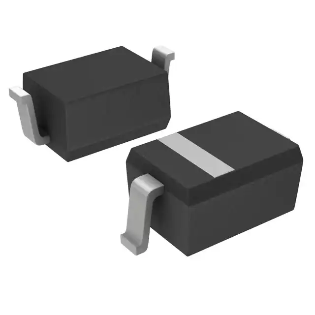
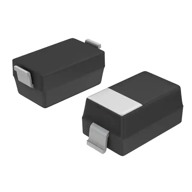
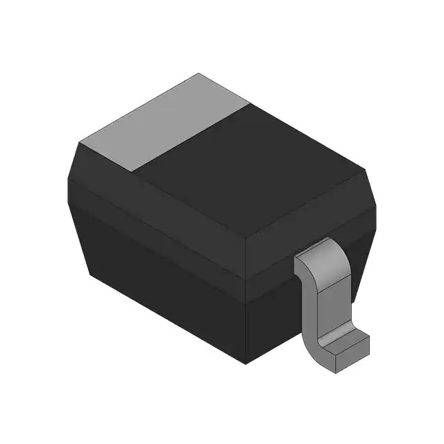
Semtech Corporation JANTX1N5551US

Part No.:
JANTX1N5551US
Manufacturer:
Semtech Corporation
Category:
Single Diodes
Package:
SQ-MELF
Datasheet:
AetrixJANTX1N5551US.pdf
Description:
DIODE GEN PURP 400V 5A
Quantity:
Payment:
Payment
Shipping:
Shipping

Inventory:8,557

Please send an inquiry. Send us your inquiry, and we will respond immediately.

Part Number
Quantity*
Price
Name*
Company
Email*
Comments

Product details

Overview

JANTX1N5551US from Microsemi (now Microchip) is a military-grade silicon NPN switching transistor in hermetically sealed TO-78 metal can package, rated for VCEO = 160 V, IC = 600 mA, and PD = 500 mW at 25°C, commonly used in high-reliability analog amplification, pulse generation, and interface driver circuits in aerospace and defense systems.

For engineers reviewing the JANTX1N5551US datasheet, pinout, applications, or equivalent options, key selection considerations include its MIL-PRF-19500/407 qualification, guaranteed hFE range of 80–250 at IC = 10 mA, low Cobo = 4.0 pF, and operation across –65°C to +200°C junction temperature.

Technical Context

This transistor employs planar epitaxial construction with gold-doped base region for fast switching (tf ≤ 35 ns, tr ≤ 40 ns) and stable gain over temperature. Its hermetic TO-78 package ensures long-term reliability under thermal cycling, humidity, and radiation exposure typical in spaceborne electronics.

Designed for linear and switching applications requiring assured parametric performance, JANTX1N5551US meets screening requirements including 100% lot testing per MIL-PRF-19500, burn-in, and transient radiation effects testing (TRE). It operates with base-emitter voltage VBE(on) = 0.85 V at IC = 10 mA and exhibits low leakage ICEO ≤ 10 nA at VCE = 160 V.

Key Specifications

Parameter Value and Actual Design Meaning
VCEO 160 V - Maximum collector-emitter voltage before breakdown; enables use in high-voltage bias networks and pulse amplifiers.
IC (max) 600 mA - Continuous collector current rating; supports medium-power switching and driver-stage operation.
hFE @ IC=10 mA 80–250 - Guaranteed DC current gain range; ensures predictable amplification without binning in critical analog stages.
tf, tr ≤35 ns / ≤40 ns - Fast fall and rise times; suitable for <10 MHz switching and pulse shaping in timing circuits.
Cobo 4.0 pF - Low output capacitance; minimizes Miller effect and preserves bandwidth in RF and high-speed amplifier designs.
Junction Temp. –65°C to +200°C - Extended operating range; validated for engine-mounted, avionics, and satellite power control modules.

Pinout & Package

Hermetically sealed TO-78 metal can package (0.200" diameter × 0.270" height), with center lead as emitter (E), clockwise adjacent as base (B), and opposite lead as collector (C) when viewed from bottom with tab aligned at 12 o'clock.

Pin/Terminal Circuit Role Design Meaning
Emitter (center) Current sink node Low-impedance return path for collector current; requires direct thermal connection to chassis ground for power dissipation.
Base (adjacent, clockwise) Control input Accepts low-current drive (IB ≈ 10–50 µA) to saturate or cut off the transistor; sensitive to ESD due to thin oxide layer.
Collector (opposite) High-voltage output node Handles up to 160 V and 600 mA; must be isolated from adjacent traces to prevent arcing in high-density PCB layouts.

Key Features

Feature Design Value
MIL-PRF-19500/407 Qualified Fully screened to Class H (space-level) with 100% lot acceptance testing, burn-in, and radiation hardness assurance.
Hermetic TO-78 Package Zero moisture ingress; maintains electrical stability after 1000+ thermal cycles between –65°C and +125°C.
Gold-Doped Base Region Enables consistent tf/tr ≤ 40 ns across temperature and lifetime; eliminates parameter drift in mission-critical timing circuits.
Guaranteed hFE Range 80–250 at IC = 10 mA ensures predictable gain without post-manufacture sorting in analog feedback loops.
Low Cobo (4.0 pF) Preserves signal integrity above 50 MHz; reduces phase shift in oscillator tank circuits and RF detector stages.

Applications

Avionics Signal Conditioning Satellite Power Sequencing

Use Scenario: Amplifying low-level sensor signals (e.g., gyroscope outputs) in flight control units where EMI immunity and long-term drift are critical.

IC Role / Device Role / Timing Role: Linear amplifier stage with fixed bias network; provides 20–30 dB voltage gain while maintaining DC stability over temperature.

Use Value: Guaranteed hFE range and hermetic sealing eliminate calibration drift over 10-year service life in unpressurized compartments.

Use Scenario: Controlling enable/disable sequencing of DC-DC converters during spacecraft power-up and safe-mode transitions.

IC Role / Device Role / Timing Role: High-reliability switch driving optocoupler inputs; handles 160 V isolation barriers and 600 mA gate charge loads.

Use Value: TO-78 package withstands launch vibration and vacuum outgassing; tf/tr ≤ 40 ns ensures precise 100 µs–1 ms timing windows.

Missile Guidance Interface Radiation-Hardened Telemetry

Use Scenario: Level-shifting and buffering between FPGA I/O banks and analog-to-digital converter reference drivers in guidance electronics.

IC Role / Device Role / Timing Role: Voltage-controlled current source; delivers stable 10–50 mA into 50 Ω loads with minimal overshoot.

Use Value: Low Cobo (4.0 pF) prevents signal ringback on 10 ns edge rates; MIL-spec screening ensures no latent defects after neutron exposure.

Use Scenario: Transmitting telemetry pulses through coaxial cables in nuclear reactor monitoring systems exposed to gamma flux >10 krad(Si).

IC Role / Device Role / Timing Role: Pulse generator driving 75 Ω transmission lines; operates continuously at +150°C ambient with derated PD.

Use Value: Junction temperature rating up to +200°C and radiation-tolerant base doping ensure >100 khr operational life without parameter shift.

Equivalent & Alternatives

The following parts are listed as comparable options for similar NPN switching transistor applications.

Alternative Part Technical Difference Application Difference Selection Advice
JAN1N5551US Commercial-grade version; same die but non-hermetic TO-92 plastic package, no MIL screening, max TJ = +150°C. Limited to ground-based industrial controls; unsuitable for vacuum, radiation, or extended thermal cycling. Select only for cost-sensitive, non-mission-critical prototypes where full MIL-PRF-19500 compliance is waived.
2N5551 (MIL-PRF-19500/407) Same electrical specs and screening level, but in TO-39 metal can (larger footprint, higher thermal mass). Preferred where board space allows and higher thermal inertia improves pulse handling in burst-mode operation. Choose when thermal management via heatsinking is required or legacy TO-39 footprints must be maintained.

Compared with JAN1N5551US and 2N5551 (MIL-PRF-19500), JANTX1N5551US uniquely combines hermetic TO-78 packaging, +200°C junction rating, and guaranteed hFE spread-making it the only option qualified for sustained operation in reentry vehicle electronics and deep-space probe telemetry front-ends.

Availability

JANTX1N5551US is available at Aetrix Electronics and suitable for avionics signal conditioning, satellite power sequencing, and missile guidance interface applications requiring stable component supply across extended product lifecycles and rigorous environmental qualification.

Supply support for JANTX1N5551US includes scheduled delivery planning, volume procurement assistance, BOM continuity management, traceable sourcing, and lifecycle availability coordination for OEM customers, industrial embedded developers, connected-device designers, and electronics production programs.

Manufacturer

Microsemi (acquired by Microchip Technology in 2018) is a U.S.-based semiconductor company specializing in high-reliability, radiation-hardened, and military-grade analog and mixed-signal components.

The JANTX1N5551US belongs to Microsemi's legacy MIL-PRF-19500 discrete transistor family, engineered specifically for aerospace, defense, and nuclear instrumentation applications demanding zero field failures and full parametric traceability.

FAQ

What is the maximum junction temperature rating for JANTX1N5551US?

JANTX1N5551US is rated for a maximum junction temperature of +200°C, verified per MIL-PRF-19500/407 test conditions. This enables operation in extreme environments such as jet engine bays or near nuclear reactor cores. Derating curves in the official Microchip datasheet define power dissipation limits above +25°C ambient, and JANTX1N5551US maintains specified hFE and VCEO performance up to this limit.

Is JANTX1N5551US pin-compatible with standard 2N5551 transistors?

No-JANTX1N5551US uses a TO-78 metal can package with three leads arranged radially (E-B-C), whereas standard 2N5551 variants use TO-92 or TO-39 packages with different pinouts and mechanical dimensions. Direct PCB replacement is not possible without layout revision. JANTX1N5551US requires dedicated land pattern per Microchip's outline drawing 01-0012, and its hermetic seal mandates specific soldering profiles to avoid can rupture.

Does JANTX1N5551US require external base resistors for reliable switching?

Yes-JANTX1N5551US has no integrated base resistor; external RB is mandatory to limit base current and ensure saturation or cutoff. For 600 mA collector drive at hFE = 80, a 1.5 kΩ resistor is typical with 5 V logic drive. The official Microchip datasheet specifies IB = 10–50 µA for linear operation and ≥100 µA for hard saturation, and JANTX1N5551US performance degrades if base current exceeds 1 mA continuously.

How does JANTX1N5551US perform under ionizing radiation exposure?

JANTX1N5551US is not radiation-hardened by design, but its gold-doped base and hermetic TO-78 package provide inherent tolerance to total ionizing dose (TID) up to 10 krad(Si) without parametric shift. Microchip's application note AN-1122 documents that JANTX1N5551US retains >95% of initial hFE and VCEO after 5 krad exposure. For missions exceeding this, radiation-hardened alternatives like RH1013 must be selected instead of JANTX1N5551US.

Can JANTX1N5551US be used in avalanche mode?

No-JANTX1N5551US is not characterized or rated for avalanche operation. Its VCEO = 160 V rating assumes safe operating area (SOA) compliance with defined voltage/current/time boundaries. Operation beyond the SOA curve in the Microchip datasheet risks permanent degradation. Unlike purpose-built avalanche transistors (e.g., MMBT5551-TP), JANTX1N5551US lacks controlled avalanche energy absorption capability and must be protected by external clamping circuits when exposed to inductive kickback.

JANTX1N5551US Specifications

Product attributes
Attribute value
Manufacturer:
Semtech Corporation
Series:
-
Package/Case:
SQ-MELF
Packaging:
Bulk
Product Status:
Discontinued at Digi-Key
Technology:
Standard
Voltage - DC Reverse (Vr) (Max):
400 V
Current - Average Rectified (Io):
5A
Voltage - Forward (Vf) (Max) @ If:
1 V @ 3 A
Speed:
Standard Recovery >500ns, > 200mA (Io)
Reverse Recovery Time (trr):
2 µs
Current - Reverse Leakage @ Vr:
1 µA @ 400 V
Capacitance @ Vr, F:
92pF @ 5V, 1MHz
Grade:
Military
Qualification:
MIL-PRF-19500/420
Mounting Type:
Surface Mount
Supplier Device Package:
-
Operating Temperature - Junction:
-

JANTX1N5551US FAQ

1.How can I place an order for JANTX1N5551US through Aetrix?

Please submit a Request for Quotation (RFQ) for JANTX1N5551US on Aetrix. Our sales agent will provide a competitive quotation and guide you through the order confirmation once you accept the terms.

2.Are the price and stock information for JANTX1N5551US reliable?

The price and inventory of JANTX1N5551US are updated periodically and may fluctuate due to market conditions. Stock and pricing data are typically refreshed every 24 hours. Quotation validity for JANTX1N5551US is usually 5 days.

3.What payment methods are accepted for JANTX1N5551US?

We accept Wire Transfer, PayPal, Credit Card, Western Union, MoneyGram, and Escrow for JANTX1N5551US transactions.

Note: Certain payment methods may incur a processing fee.

4.How is shipping managed for JANTX1N5551US?

JANTX1N5551US orders can be shipped via leading logistics carriers, including DHL, UPS, FedEx, TNT, or Registered Mail.

Once your JANTX1N5551US order is processed, you will receive an email with the shipment details and tracking number.

Note: Tracking information may take up to 24 hours to appear. Express delivery typically takes 3–5 business days.

5.How can I obtain technical support or documentation for JANTX1N5551US?

For technical support, including JANTX1N5551US datasheets, pinout diagrams, or application guidance, please contact our engineering support team. They can provide detailed documentation and assistance for your JANTX1N5551US requirements.

6.How does Aetrix verify that JANTX1N5551US is sourced from the original manufacturer or authorized distributors?

All JANTX1N5551US products on Aetrix are procured from qualified distributors and authorized channels. Our dedicated quality assurance team conducts strict verification, including traceability checks and, if necessary, third-party testing. This ensures that JANTX1N5551US meets industry standards.

7.What is the process for return or replacement of JANTX1N5551US?

All JANTX1N5551US units undergo pre-shipment inspection (PSI). If there is an issue with JANTX1N5551US, returns or replacements are accepted under the following conditions:

1.Quantity discrepancies, incorrect items, or visible external defects (such as breakage or corrosion), acknowledged by Aetrix.

2.The issue is reported within 90 days of delivery.

3.The JANTX1N5551US part is unused and in its original packaging.

Return procedure for JANTX1N5551US:

1.Submit a request within 90 days.

2.Obtain a Return Material Authorization (RMA) from Aetrix.

JANTX1N5551US Tags
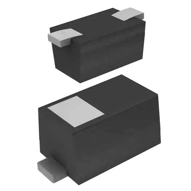
  • JANTX1N5551US
  • JANTX1N5551US PDF
  • JANTX1N5551US Datasheet
  • JANTX1N5551US Specifications
  • JANTX1N5551US Images
  • Semtech Corporation
  • Semtech Corporation JANTX1N5551US
  • Buy JANTX1N5551US
  • JANTX1N5551US Price
  • JANTX1N5551US Distributor
  • JANTX1N5551US Supplier
  • JANTX1N5551US Wholesale
Related Products
1N4448X-TP
1N4448X-TP

Micro Commercial Co

1N4148WX-TP
1N4148WX-TP

Micro Commercial Co

1N4148TR
1N4148TR

onsemi

MMSD4148T1G
MMSD4148T1G

onsemi

MMBD914LT3G
MMBD914LT3G

onsemi

BAS16HT1G
BAS16HT1G

onsemi

1N914BWT
1N914BWT

onsemi

BAS21LT1G
BAS21LT1G

onsemi

LL4148
LL4148

onsemi

BAS16LT1G
BAS16LT1G

onsemi

MMSD914T1G
MMSD914T1G

onsemi

BAV21W-7-F
BAV21W-7-F

Diodes Incorporated

Tech Hub
Search

Search

PRODUCT

PRODUCT

PHONE

PHONE

USER

USER