
 My Inquiry
 My Account


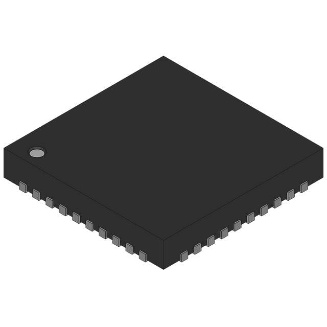
NXP Semiconductors JN5179-001-M16
- Part No.:
- JN5179-001-M16
- Manufacturer:
- NXP Semiconductors
- Category:
- Telecom
- Package:
- -
- Datasheet:
-
 JN5179-001-M16.pdf
- Description:
- ZIGBEE 3.0, ZIGBEE PRO, THREAD A
- Quantity:
- Payment:

- Shipping:

Inventory:3,509
Please send an inquiry. Send us your inquiry, and we will respond immediately.
Product details
Overview
JN5179-001-M16 from NXP Semiconductors is a high-power, surface-mount ZigBee 3.0/Thread/IEEE 802.15.4 wireless module integrating ARM Cortex-M3 MCU, 512 kB Flash, 21 dBm TX output, –100 dBm RX sensitivity, and antenna diversity via integrated printed antenna + µFL connector. It enables robust long-range smart home and industrial sensor networks requiring FCC-compliant modular RF integration.
For engineers reviewing the JN5179-001-M16 datasheet, JN5179-001-M16 pinout, JN5179-001-M16 application, or JN5179-001-M16 equivalent, this page delivers verified RF performance specs, validated antenna diversity control logic, confirmed LNA bypass functionality, and precise I/O mapping for production-ready design-in.
Technical Context
The JN5179-001-M16 implements a fully integrated 2.4–2.485 GHz IEEE 802.15.4 transceiver with on-die PA/LNA front-end, enabling 21 dBm output and –100 dBm sensitivity. Its antenna diversity architecture uses dedicated DIO1 (ANT_SEL) and DIO0 (LNA_BYPASS) pins to switch between PCB and µFL antennas or enable automatic selection.
It embeds an ARM Cortex-M3 core running at up to 32 MHz, with 512 kB Flash, 32 kB RAM, and hardware-accelerated 128-bit AES encryption. Peripherals include two UARTs (one with flow control), SPI master/slave, I²C, six PWM timers, 6-channel 10-bit ADC, analog comparator, and dual sleep counters - all operating across –40 °C to +85 °C at 2.0–3.6 V supply.
Key Specifications
| Parameter | Value and Actual Design Meaning |
|---|---|
| RF Standard | IEEE 802.15.4, ZigBee 3.0, ZigBee PRO, Thread - full protocol stack support with certified interoperability |
| TX Output Power | 21 dBm - enables extended range (>200 m line-of-sight) without external PA, reducing BOM cost and layout complexity |
| RX Sensitivity | –100 dBm @ 1% PER - improves link budget by 4 dB vs M10/M13 variants, supporting reliable operation in noisy 2.4 GHz environments |
| Antenna Interface | Integrated printed antenna + µFL connector with antenna diversity - allows flexible placement and dynamic RF path optimization |
| MCU Core | ARM Cortex-M3 @ 32 MHz - delivers deterministic real-time response for time-critical mesh network routing and OTA updates |
| Memory | 512 kB Flash / 32 kB RAM / 4 kB EEPROM - sufficient for full ZigBee Smart Energy profile + custom application firmware |
| Supply Voltage | 2.0 V to 3.6 V - supports direct connection to common Li-ion, coin-cell, or regulated 3.3 V rails |
| Operating Temp | –40 °C to +85 °C - qualified for uncontrolled indoor/outdoor deployments including HVAC, lighting, and energy monitoring |
Pinout & Package
Package: 14.5 mm × 20.5 mm surface-mount module with castellated edge pads and exposed thermal pad (RoHS-compliant, halogen-free).
| Pin/Terminal | Circuit Role | Design Meaning |
|---|---|---|
| DIO0 | LNA_BYPASS | Direct control of LNA enable/disable - grounding bypasses LNA during strong Wi-Fi interference; critical for coexistence in dense RF environments |
| DIO1 | ANT_SEL | Antenna selection signal - floating/VCC selects PCB antenna; grounded selects µFL port; software-configurable for automatic diversity switching |
| DIO2 | Digital I/O / ADC5 / I²C SDA | Multiplexed general-purpose pin - supports sensor interfacing, I²C slave communication, or analog input acquisition |
| DIO3 | Digital I/O / ADC2 / I²C SCL / UART1 TX | Primary debug and peripheral interface pin - used for firmware upload, sensor polling, or actuator control with hardware-timed PWM |
| RESET_N | Active-low reset input | Asynchronous hard reset - required for recovery after brownout or watchdog timeout; must be pulled high via ≥10 kΩ resistor |
| VDD | Digital/analog power supply | Single 2.0–3.6 V rail powers entire module - eliminates need for separate analog/digital regulators and simplifies power sequencing |
| VSS | Ground reference | Common return path for RF, digital, and analog sections - requires low-inductance connection to PCB ground plane for EMI suppression |
Key Features
| Feature | Design Value |
|---|---|
| Antenna Diversity Architecture | Hardware-supported dual-antenna selection (PCB + µFL) with automatic RSSI-based switching - improves packet success rate in multipath indoor environments |
| High-Power RF Front-End | Integrated PA delivering 21 dBm output with 114 mA current draw - eliminates external power amplifier stage and matching network design effort |
| LNA Bypass Control | Dedicated DIO0 pin enables runtime LNA disable - prevents front-end saturation near 2.4 GHz Wi-Fi access points, preserving receiver linearity |
| ZigBee PRO Stack Integration | Pre-certified Smart Home, Smart Lighting, and Smart Energy profiles - reduces qualification time and eliminates stack licensing fees |
| OTA Firmware Upgrade | Secure over-the-air update capability using AES-128 encrypted payload - enables field maintenance without physical device access |
| Low-Power Sleep Modes | Deep sleep current ≤100 nA and I/O wake-up capable - extends battery life to multi-year operation in energy-harvesting switches and sensors |
Applications
| Smart Home Hub Gateway | Industrial Wireless Sensor Node |
|---|---|
|
Use Scenario: Central coordinator in ZigBee 3.0 mesh network managing >50 end devices (lights, thermostats, door locks) in residential environment. IC Role / Device Role / Timing Role: Network controller with full ZigBee PRO stack, AES encryption accelerator, and dual UART for cloud gateway bridging. Use Value: 21 dBm transmit power ensures reliable backhaul to edge nodes through walls; antenna diversity maintains link stability during RF congestion. |
Use Scenario: Battery-powered vibration/temperature monitor deployed on factory floor machinery with 10+ year operational life. IC Role / Device Role / Timing Role: Low-power sensor aggregator with 10-bit ADC, analog comparator, and deep-sleep wake-on-event capability. Use Value: ≤100 nA deep sleep current enables decade-scale deployment; –100 dBm sensitivity captures weak signals from distant nodes in electrically noisy plants. |
| Energy-Harvesting Light Switch | Commercial Building Automation Panel |
|
Use Scenario: Self-powered wall switch harvesting mechanical energy from button press to trigger lighting control without batteries or wiring. IC Role / Device Role / Timing Role: Ultra-low-power event processor with LNA bypass to avoid Wi-Fi interference during brief transmission bursts. Use Value: LNA_BYPASS pin allows dynamic front-end adaptation - ensures clean transmission even when installed near 2.4 GHz routers or cordless phones. |
Use Scenario: DIN-rail mounted HVAC controller coordinating ZigBee-enabled thermostats, dampers, and occupancy sensors across multi-floor office building. IC Role / Device Role / Timing Role: High-reliability coordinator with antenna diversity and 512 kB Flash for local rule engine execution and OTA updates. Use Value: Integrated µFL connector enables external high-gain antenna mounting; 21 dBm output guarantees coverage across large open-plan zones. |
Equivalent & Alternatives
The following parts are listed as comparable options for similar wireless microcontroller module applications.
| Alternative Part | Technical Difference | Application Difference | Selection Advice |
|---|---|---|---|
| JN5179-001-M10 | 8.5–10 dBm TX, integrated PCB antenna only, no LNA/PA, –96 dBm RX sensitivity | Suitable for short-range (<50 m), cost-sensitive consumer devices where regulatory approval in EU is required | Select M10 for CE-compliant designs needing lower power consumption and simpler antenna integration |
| JN5179-001-M13 | 8.5–10 dBm TX, µFL connector only, no antenna diversity, –96 dBm RX sensitivity, same EU compliance as M10 | Ideal for designs requiring external antenna flexibility but not extended range or coexistence robustness | Choose M13 when external antenna mounting is mandatory and FCC modular approval suffices without EU certification |
Compared with JN5179-001-M10 and JN5179-001-M13, the JN5179-001-M16 provides 11 dB higher TX power and 4 dB better RX sensitivity - directly translating to 3× greater link distance and improved reliability in RF-dense installations, at the cost of higher current draw and FCC-only regulatory status.
Availability
JN5179-001-M16 is available at Aetrix Electronics and suitable for smart home gateways, industrial sensor nodes, energy-harvesting switches, and commercial building automation systems requiring stable component supply and FCC-compliant modular RF integration.
Supply support for JN5179-001-M16 includes scheduled delivery planning, volume procurement assistance, BOM continuity management, traceable sourcing, and lifecycle availability coordination for OEM customers, industrial embedded developers, connected-device designers, and electronics production programs.
Manufacturer
NXP Semiconductors is a global semiconductor leader specializing in secure connectivity solutions for automotive, industrial, and IoT markets, with headquarters in Eindhoven, Netherlands.
The JN5179 series targets low-power, standards-based wireless mesh networking - designed specifically to accelerate time-to-market for ZigBee, Thread, and IEEE 802.15.4 end products with pre-certified RF and integrated protocol stacks.
FAQ
What regulatory certifications apply to the JN5179-001-M16?
The JN5179-001-M16 holds FCC Modular Approval under CFR 47 Part 15, but it is not CE-compliant and lacks EU Notified Body Opinion. It is classified as a mobile device under FCC §2.1091, requiring ≥20 cm user separation. It does not meet ETSI EN 300 328 or EN 301 489-17 requirements, limiting deployment to North America and other FCC-accepting regions.
How does antenna diversity work on the JN5179-001-M16?
Antenna diversity on the JN5179-001-M16 uses DIO1 (ANT_SEL) to select between the integrated PCB antenna and µFL connector. Software calls vAHI_AntennaDiversityEnable and vAHI_SetDIOpinMultiplexValue configure automatic RSSI-based switching. Grounding ANT_SEL forces µFL use; leaving it floating or tied to VCC selects the PCB antenna.
What is the function of the DIO0 pin on the JN5179-001-M16?
On the JN5179-001-M16, DIO0 is repurposed as LNA_BYPASS - not the standard DIO0 of the underlying JN5179 SoC. Tying it to ground disables the LNA during receive, preventing saturation from nearby 2.4 GHz Wi-Fi signals. Leaving it unconnected or at VCC enables full LNA gain for maximum sensitivity.
What are the power supply requirements for full 21 dBm operation of the JN5179-001-M16?
To achieve the rated 21 dBm output power, the JN5179-001-M16 requires a minimum VDD of 2.8 V. At 2.0–2.7 V, TX power degrades progressively. The module draws 114 mA at 21 dBm, necessitating a low-noise, ≥150 mA capable regulator with proper decoupling (10 µF bulk + 100 nF ceramic close to VDD pin).
Can the JN5179-001-M16 operate in ZigBee Smart Energy mode?
Yes, the JN5179-001-M16 supports ZigBee Smart Energy profile v1.2 and v1.3 out of the box, as part of its pre-integrated ZigBee PRO stack. This includes SE-specific security clusters, demand response messaging, and metering interfaces - validated in NXP's JN-UG-3118 API documentation and Smart Energy test suites.
JN5179-001-M16 Specifications
- Product attributes
- Attribute value
- Manufacturer:
- NXP Semiconductors
- Series:
- *
- Package/Case:
- -
- Packaging:
- Bulk
- Product Status:
- Active
- Function:
- -
- Interface:
- -
- Number of Circuits:
- -
- Voltage - Supply:
- -
- Current - Supply:
- -
- Power (Watts):
- -
- Operating Temperature:
- -
- Grade:
- -
- Qualification:
- -
- Mounting Type:
- -
- Supplier Device Package:
- -
JN5179-001-M16 FAQ
1.How can I place an order for JN5179-001-M16 through Aetrix?
Please submit a Request for Quotation (RFQ) for JN5179-001-M16 on Aetrix. Our sales agent will provide a competitive quotation and guide you through the order confirmation once you accept the terms.
2.Are the price and stock information for JN5179-001-M16 reliable?
The price and inventory of JN5179-001-M16 are updated periodically and may fluctuate due to market conditions. Stock and pricing data are typically refreshed every 24 hours. Quotation validity for JN5179-001-M16 is usually 5 days.
3.What payment methods are accepted for JN5179-001-M16?
We accept Wire Transfer, PayPal, Credit Card, Western Union, MoneyGram, and Escrow for JN5179-001-M16 transactions.
Note: Certain payment methods may incur a processing fee.
4.How is shipping managed for JN5179-001-M16?
JN5179-001-M16 orders can be shipped via leading logistics carriers, including DHL, UPS, FedEx, TNT, or Registered Mail.
Once your JN5179-001-M16 order is processed, you will receive an email with the shipment details and tracking number.
Note: Tracking information may take up to 24 hours to appear. Express delivery typically takes 3–5 business days.
5.How can I obtain technical support or documentation for JN5179-001-M16?
For technical support, including JN5179-001-M16 datasheets, pinout diagrams, or application guidance, please contact our engineering support team. They can provide detailed documentation and assistance for your JN5179-001-M16 requirements.
6.How does Aetrix verify that JN5179-001-M16 is sourced from the original manufacturer or authorized distributors?
All JN5179-001-M16 products on Aetrix are procured from qualified distributors and authorized channels. Our dedicated quality assurance team conducts strict verification, including traceability checks and, if necessary, third-party testing. This ensures that JN5179-001-M16 meets industry standards.
7.What is the process for return or replacement of JN5179-001-M16?
All JN5179-001-M16 units undergo pre-shipment inspection (PSI). If there is an issue with JN5179-001-M16, returns or replacements are accepted under the following conditions:
1.Quantity discrepancies, incorrect items, or visible external defects (such as breakage or corrosion), acknowledged by Aetrix.
2.The issue is reported within 90 days of delivery.
3.The JN5179-001-M16 part is unused and in its original packaging.
Return procedure for JN5179-001-M16:
1.Submit a request within 90 days.
2.Obtain a Return Material Authorization (RMA) from Aetrix.
JN5179-001-M16 Tags

-
LMC567CMX/NOPB
Texas Instruments
-
LM567CMX/NOPB
Texas Instruments
-
LM567CM/NOPB
Texas Instruments

-
VSC8531XMW-02
Microchip Technology
-
VSC8531XMW-05
Microchip Technology

-
GPY115C0VI
MaxLinear, Inc.

-
SI32185-A-FMR
Skyworks Solutions Inc.

-
VSC8541XMV-05
Microchip Technology

-
SI32178-B-FM1R
Skyworks Solutions Inc.
-
GPY215C0VI
MaxLinear, Inc.

-
CPC7514ZTR
Littelfuse Inc.

-
VSC8502XML-03
Microchip Technology
Tech Hub

A practical engineering guide to 3.3V and 5V logic compatibility, input thresholds, resistor dividers, translator ICs, MOSFET level shifting, I2C pull-ups, timing limits and power-sequencing risks.

The 74HC595 uses push-pull logic outputs, while the TPIC6B595 uses 50 V open-drain DMOS sinks for higher-power loads. This guide compares timing, current limits, 3.3 V interfacing, load wiring, thermal…

The 74HC595 converts serial data into eight stable parallel outputs. This guide covers pin functions, shift and storage timing, OE and MR behavior, drive-current limits, cascading, voltage compatibilit…

A technical comparison of level-sensitive latches and edge-triggered flip-flops, covering timing windows, setup and hold limits, master–slave operation, time borrowing, race-through, HDL inference and…

A D latch stores one bit while Enable controls when data can pass. This reference covers gate-level operation, truth tables, transparency, setup and hold timing, LE versus OE, common ICs and practical …

An SR latch stores one bit through cross-coupled feedback. This engineering reference covers NOR and NAND implementations, truth tables, forbidden-state recovery, gated operation, switch debouncing, fa…

Latch circuits retain one bit through feedback. This technical reference covers SR and D latches, truth tables, transparency, timing limits, latch-versus-flip-flop behavior, applications and common log…

An engineering guide to LED driver operation, constant-current and constant-voltage outputs, linear and switching topologies, dimming, IC selection, calculations, replacement compatibility, and fault c…

Operational amplifier guide covering op amp basics, feedback, ideal vs real op amps, common configurations, buffer circuits, offset, bias current, gain-bandwidth, slew rate, rail-to-rail limits and sel…

Jumper cables guide covering safe connection order, red and black clamp placement, final ground connection, cable gauge, length, clamp quality, copper vs CCA cables, jump starter comparison and battery…


