
 My Inquiry
 My Account


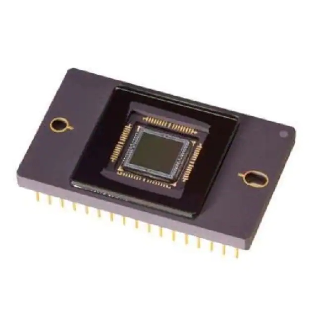
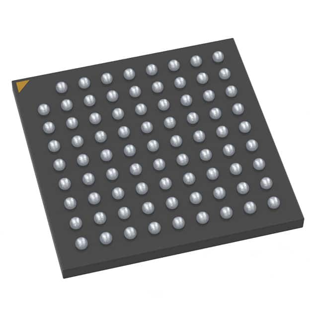
onsemi KAI-01050-ABA-JD-BA
- Part No.:
- KAI-01050-ABA-JD-BA
- Manufacturer:
- onsemi
- Category:
- Image Sensors, Camera
- Package:
- 67-BCPGA
- Datasheet:
-
 KAI-01050-ABA-JD-BA.pdf
- Description:
- IMAGE SENSOR CCD 1MP 67CPGA
- Quantity:
- Payment:

- Shipping:

Inventory:3,090
Please send an inquiry. Send us your inquiry, and we will respond immediately.
Product details
Overview
KAI-01050-ABA-JD-BA from onsemi is a monochrome 1024 × 1024 interline transfer CCD image sensor in 68-pin PGA package, featuring 5.5 µm pixels, 64 dB dynamic range, 12 e⁻ rms read noise at 40 MHz, and support for quad/dual/single output readout up to 120/60/30 fps - deployed in high-precision industrial inspection systems requiring low smear (−100 dB) and blooming suppression (>300×).
For engineers reviewing the KAI-01050-ABA-JD-BA datasheet, pinout, applications, or equivalent options, this page delivers verified technical context, exact pin functions per quadrant, real-world imaging performance metrics, and validated alternative sensors for monochrome machine vision designs operating under controlled thermal and timing conditions.
Technical Context
The KAI-01050-ABA-JD-BA implements a progressive-scan interline CCD architecture with vertical overflow drain for electronic shuttering and blooming control. Its four-quadrant readout enables parallel analog output paths (VOUTa–d), each with dedicated reset gates (Ra–d), output gates (OGa–d), and horizontal/vertical clock domains (H1S/H2S/V1B–V4T).
Each quadrant uses independent 5.5 µm × 5.5 µm photodiodes with 20,000 e⁻ charge capacity and shares common substrate (SUB) and ESD disable (ESD) terminals. Pixel-level dark reference columns (22 left/right) and dummy rows (1 top/bottom + 12 top/bottom dark rows) support calibrated offset correction without requiring external black-level circuitry.
Key Specifications
| Parameter | Value and Actual Design Meaning |
|---|---|
| Resolution | 1024 (H) × 1024 (V) active pixels - full-frame area of 5.632 mm × 5.632 mm, 1/2″ optical format suitable for C-mount lenses. |
| Read Noise | 12 e⁻ rms at 40 MHz pixel clock - enables high-fidelity digitization of low-light signals without amplification-induced quantization penalty. |
| Dynamic Range | 64 dB - supports simultaneous capture of high-contrast scenes (e.g., laser-illuminated metal surfaces with specular highlights and shadowed features). |
| Smear Performance | −100 dB - ensures minimal vertical signal corruption during fast exposure transitions in moving-part inspection. |
| Blooming Suppression | >300× - prevents charge spillage from saturated pixels into adjacent regions, critical for defect detection in bright-field AOI. |
| Frame Rate | 120 fps (quad-output), 60 fps (dual-output), 30 fps (single-output) - scalable bandwidth allocation for throughput vs. SNR trade-offs. |
| Quantum Efficiency | 44% peak at 480 nm - optimized for monochrome LED illumination (e.g., 530 nm green source), delivering maximum photon-to-electron conversion in visible spectrum. |
Pinout & Package
Package: 68-pin Pin Grid Array (PGA), ceramic body, clear AR-coated cover glass (both sides), telecentric microlens array, standard grade.
| Pin | Circuit Role | Design Meaning |
|---|---|---|
| 1, 33, 35, 67 | V3B / V3T | Vertical CCD clock phase 3 (bottom/top) - controls charge transfer timing in vertical shift register; must be driven with precise 0–12 V swing and <1 ns edge rate. |
| 8, 28, 42, 62 | VOUTa–d | Analog video output per quadrant - differential-capable, 127 Ω output impedance, DC-coupled, requires 9.4 V DC offset for proper ADC interfacing. |
| 9, 25, 43, 59 | Ra–d | Reset gate per quadrant - initiates pixel reset before integration; driven with −2.0 V nominal to control dark current injection. |
| 11, 23, 45, 57 | H2SLa–d | Horizontal CCD clock phase 2, storage, last - final horizontal transfer pulse before output gate opening; timing-critical for smear minimization. |
| 34, 68 | ESD | ESD protection disable - pulled to −9.0 V to deactivate internal clamps; required before power-up to prevent latch-up during bias sequencing. |
| 36 | DevID | Device identification - open-drain output used to verify sensor presence and version during system initialization. |
Key Features
| Feature | Design Value |
|---|---|
| Quad-output flexible readout | Enables 120 fps full-resolution capture or selectable dual/single mode for reduced data bandwidth and lower system power consumption. |
| Electronic shutter with overflow drain | Provides precise exposure control down to microsecond resolution without mechanical components - essential for synchronized flash triggering in production lines. |
| Low-smear architecture | −100 dB smear level eliminates vertical streaking artifacts during rapid motion capture, enabling reliable OCR and PCB trace inspection. |
| On-chip dark reference columns | 22 shielded columns per side supply real-time black-level calibration, reducing need for external offset compensation circuitry and improving temperature stability. |
| Telecentric microlens array | Maximizes angular quantum efficiency across ±10° field of view - maintains uniform responsivity for off-axis light in lens-coupled industrial optics. |
Applications
| Industrial Machine Vision | Medical Endoscopy Imaging |
|---|---|
Use Scenario: High-speed automated optical inspection (AOI) of printed circuit boards with laser line illumination and sub-pixel registration. IC Role / Device Role / Timing Role: Primary image capture device; provides synchronized frame-triggered exposure and quad-channel analog output for FPGA-based real-time defect analysis. Use Value: 120 fps full-resolution operation enables 100% inline coverage at conveyor speeds >2 m/s; −100 dB smear prevents false positives from moving solder joints. | Use Scenario: Rigid endoscope for minimally invasive surgery requiring high-fidelity grayscale imaging under pulsed LED illumination. IC Role / Device Role / Timing Role: Monochrome image sensor capturing 1024 × 1024 frames at 60 fps with electronic shutter synchronization to LED pulses. Use Value: 44% peak QE at 480 nm maximizes photon collection from blue-enhanced surgical LEDs; 64 dB DR preserves detail in both tissue highlights and deep cavity shadows. |
| Security Perimeter Monitoring | Scientific Microscopy |
Use Scenario: Low-light outdoor perimeter camera using IR-cut filter switching and high-sensitivity monochrome mode at night. IC Role / Device Role / Timing Role: Light-sensitive imaging element operating in single-output mode for maximum SNR; integrates with thermoelectric cooler for dark current suppression. Use Value: 7 e⁻/s photodiode dark current at 40°C enables clean 10+ second exposures; AR-coated cover glass boosts transmission >98% across visible/NIR band. | Use Scenario: Fluorescence lifetime imaging (FLIM) setup requiring precise exposure control and minimal lag for time-gated acquisition. IC Role / Device Role / Timing Role: Time-resolved detector with electronic shutter and negligible lag (<10 e⁻); triggered by picosecond laser pulses via ESD-controlled exposure window. Use Value: Vertical overflow drain enables sub-microsecond shutter accuracy; 0.999999 CTE ensures quantitative fidelity across multi-frame intensity decay curves. |
Equivalent & Alternatives
The following parts are listed as comparable options for similar CCD image sensor applications.
| Alternative Part | Technical Difference | Application Difference | Selection Advice |
|---|---|---|---|
| KAI-01050-ABA-FD-BA | Same die, CLCC-64 package with sealed AR-coated cover glass - no PGA socket interface, different thermal mass and mounting method. | Preferred for hermetic, high-reliability modules where board-level rework is impractical; unsuitable for socket-based evaluation platforms. | Select when long-term environmental sealing and vibration resistance outweigh flexibility of PGA socket prototyping. |
| KAI-02150-ABA-JD-BA | 2.2 MP (1600 × 1200), same TRUESENSE 5.5 µm platform, identical pinout and electrical interface - higher resolution but lower max frame rate (60 fps quad). | Used in higher-resolution metrology systems where pixel count >1 MP is mandatory; requires wider data bus and increased FPGA resources. | Select when spatial resolution is prioritized over speed; retains full software/hardware compatibility except for timing and memory buffer sizing. |
Compared with KAI-01050-ABA-FD-BA, the PGA version offers socket-based prototyping and thermal management advantages; compared with KAI-02150-ABA-JD-BA, it delivers 2× higher frame rate at the cost of 55% fewer pixels - making it optimal for high-throughput, moderate-resolution inspection tasks.
Availability
KAI-01050-ABA-JD-BA is available at Aetrix Electronics and suitable for industrial machine vision, medical endoscopy, and security perimeter monitoring requiring stable component supply, long-lifecycle support, and consistent parametric performance across production batches.
Supply support for KAI-01050-ABA-JD-BA includes scheduled delivery planning, volume procurement assistance, BOM continuity management, traceable sourcing, and lifecycle availability coordination for OEM customers, industrial embedded developers, connected-device designers, and electronics production programs.
Manufacturer
onsemi (Nasdaq: ON) is a global semiconductor supplier delivering energy-efficient, intelligent power and sensing solutions for automotive, industrial, cloud, medical, and IoT applications.
The KAI-01050-ABA-JD-BA belongs to the TRUESENSE interline CCD family, engineered specifically for high-dynamic-range, low-noise monochrome imaging in factory automation and precision diagnostics where analog signal integrity and temporal accuracy are non-negotiable.
FAQ
What is the maximum frame rate achievable with KAI-01050-ABA-JD-BA in quad-output mode?
KAI-01050-ABA-JD-BA achieves 120 fps in quad-output mode at full 1024 × 1024 resolution with 40 MHz pixel clock. This requires simultaneous use of all four analog outputs (VOUTa–d), matched termination, and precise clock skew management across quadrants. Frame rate drops to 60 fps in dual-output and 30 fps in single-output configurations due to serialization overhead.
Does KAI-01050-ABA-JD-BA support electronic shuttering, and how is it implemented?
Yes, KAI-01050-ABA-JD-BA supports precise electronic shuttering via its vertical overflow drain structure. Shutter control is managed by biasing the SUB (substrate) voltage and sequencing the V1B–V4B/T clocks. The ESD pin must be stabilized before shutter pulsing, and exposure time is defined by the interval between vertical clock phases - enabling microsecond-resolution exposure control without mechanical components.
What are the key thermal considerations for stable operation of KAI-01050-ABA-JD-BA?
KAI-01050-ABA-JD-BA exhibits photodiode dark current doubling every 7°C; at 40°C it measures 7 e⁻/s, rising to ~56 e⁻/s at 61°C. Stable operation requires heatsinking or thermoelectric cooling to maintain junction temperature ≤40°C. The PGA package's thermal resistance (θJA) is 35°C/W - ambient temperature must be controlled, and power dissipation (0.4 W typical at 40 MHz quad mode) must be managed to avoid SNR degradation.
How does the dark reference structure function in KAI-01050-ABA-JD-BA, and which pixels should be used?
KAI-01050-ABA-JD-BA includes 22 dark reference columns on the left and right edges, plus 12 dark rows at top/bottom. Only the center 20 of the 22 dark columns should be used for black-level calibration due to potential light leakage at outer edges. These columns are unshielded but not exposed to scene light - their average output provides real-time offset correction without requiring external black references.
Is KAI-01050-ABA-JD-BA pin-compatible with other devices in the TRUESENSE 5.5 µm platform?
Yes, KAI-01050-ABA-JD-BA shares identical pinout and electrical configuration with all members of the TRUESENSE 5.5 µm interline CCD platform, including KAI-02150 and KAI-03400 variants. This allows single-camera hardware designs to support multiple resolutions and output configurations through firmware and timing changes - reducing development cost and time-to-market for scalable vision systems.
KAI-01050-ABA-JD-BA Specifications
- Product attributes
- Attribute value
- Manufacturer:
- onsemi
- Series:
- -
- Package/Case:
- 67-BCPGA
- Packaging:
- Bulk
- Product Status:
- Obsolete
- Type:
- CCD
- Pixel Size:
- 5.5µm x 5.5µm
- Active Pixel Array:
- 1024H x 1024V
- Frames per Second:
- 120.0
- Voltage - Supply:
- 14.5V ~ 15.5V
- Supplier Device Package:
- 67-CPGA (33.02x20.07)
- Operating Temperature:
- -50°C ~ 70°C
- Grade:
- -
- Qualification:
- -
KAI-01050-ABA-JD-BA FAQ
1.How can I place an order for KAI-01050-ABA-JD-BA through Aetrix?
Please submit a Request for Quotation (RFQ) for KAI-01050-ABA-JD-BA on Aetrix. Our sales agent will provide a competitive quotation and guide you through the order confirmation once you accept the terms.
2.Are the price and stock information for KAI-01050-ABA-JD-BA reliable?
The price and inventory of KAI-01050-ABA-JD-BA are updated periodically and may fluctuate due to market conditions. Stock and pricing data are typically refreshed every 24 hours. Quotation validity for KAI-01050-ABA-JD-BA is usually 5 days.
3.What payment methods are accepted for KAI-01050-ABA-JD-BA?
We accept Wire Transfer, PayPal, Credit Card, Western Union, MoneyGram, and Escrow for KAI-01050-ABA-JD-BA transactions.
Note: Certain payment methods may incur a processing fee.
4.How is shipping managed for KAI-01050-ABA-JD-BA?
KAI-01050-ABA-JD-BA orders can be shipped via leading logistics carriers, including DHL, UPS, FedEx, TNT, or Registered Mail.
Once your KAI-01050-ABA-JD-BA order is processed, you will receive an email with the shipment details and tracking number.
Note: Tracking information may take up to 24 hours to appear. Express delivery typically takes 3–5 business days.
5.How can I obtain technical support or documentation for KAI-01050-ABA-JD-BA?
For technical support, including KAI-01050-ABA-JD-BA datasheets, pinout diagrams, or application guidance, please contact our engineering support team. They can provide detailed documentation and assistance for your KAI-01050-ABA-JD-BA requirements.
6.How does Aetrix verify that KAI-01050-ABA-JD-BA is sourced from the original manufacturer or authorized distributors?
All KAI-01050-ABA-JD-BA products on Aetrix are procured from qualified distributors and authorized channels. Our dedicated quality assurance team conducts strict verification, including traceability checks and, if necessary, third-party testing. This ensures that KAI-01050-ABA-JD-BA meets industry standards.
7.What is the process for return or replacement of KAI-01050-ABA-JD-BA?
All KAI-01050-ABA-JD-BA units undergo pre-shipment inspection (PSI). If there is an issue with KAI-01050-ABA-JD-BA, returns or replacements are accepted under the following conditions:
1.Quantity discrepancies, incorrect items, or visible external defects (such as breakage or corrosion), acknowledged by Aetrix.
2.The issue is reported within 90 days of delivery.
3.The KAI-01050-ABA-JD-BA part is unused and in its original packaging.
Return procedure for KAI-01050-ABA-JD-BA:
1.Submit a request within 90 days.
2.Obtain a Return Material Authorization (RMA) from Aetrix.
KAI-01050-ABA-JD-BA Tags

-
MT9M114EBLSTCZ-CR
onsemi
-
EPC611-CSP24-001
ESPROS Photonics AG
-
AR0147ATSC00XUEG5-DRBR
onsemi
-
AR0130CSSM00SPCA0-DRBR
onsemi
-
AR1335CSSC11SMKA0-CP
onsemi
-
AR0521SR2M09SURA0-DP
onsemi
-
AR0135CS2M25SUEA0-DPBR
onsemi
-
AR0522SRSC09SURA0-DP
onsemi
-
AR0134CSSC00SPCA0-DPBR
onsemi
-
AR0134CSSM00SUEA0-DPBR
onsemi
-
AR0521SR2C09SURA0-DP
onsemi
-
AR0135CS2M00SUEA0-DPBR
onsemi
Tech Hub

Schmitt triggers use separate rising and falling thresholds to stabilize slow or noisy signals. This guide covers hysteresis, 74HC14 and 74HCT14 selection, comparator calculations, RC oscillators and p…

Counterfeit components can hide behind convincing markings and passing basic function tests. This engineering reference covers source traceability, external inspection, X-ray, XRF, electrical testing, …

A practical engineering and sourcing framework covering lifecycle verification, lifetime-buy calculations, replacement qualification, supplier checks and counterfeit-risk controls.

TTL and CMOS logic families differ in thresholds, loading, output drive, power and timing. This engineering guide compares 74HC and 74HCT, calculates noise margins and checks 3.3 V/5 V compatibility.

A practical engineering guide to 3.3V and 5V logic compatibility, input thresholds, resistor dividers, translator ICs, MOSFET level shifting, I2C pull-ups, timing limits and power-sequencing risks.

The 74HC595 uses push-pull logic outputs, while the TPIC6B595 uses 50 V open-drain DMOS sinks for higher-power loads. This guide compares timing, current limits, 3.3 V interfacing, load wiring, thermal…

The 74HC595 converts serial data into eight stable parallel outputs. This guide covers pin functions, shift and storage timing, OE and MR behavior, drive-current limits, cascading, voltage compatibilit…

A technical comparison of level-sensitive latches and edge-triggered flip-flops, covering timing windows, setup and hold limits, master–slave operation, time borrowing, race-through, HDL inference and…

A D latch stores one bit while Enable controls when data can pass. This reference covers gate-level operation, truth tables, transparency, setup and hold timing, LE versus OE, common ICs and practical …

An SR latch stores one bit through cross-coupled feedback. This engineering reference covers NOR and NAND implementations, truth tables, forbidden-state recovery, gated operation, switch debouncing, fa…


