
 My Inquiry
 My Account


NXP Semiconductors KMC7448HX1267ND
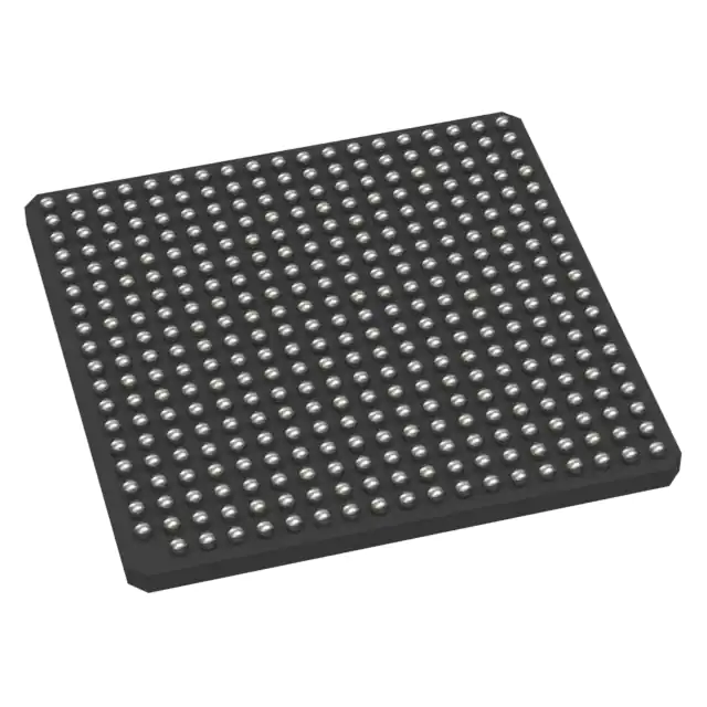
- Part No.:
- KMC7448HX1267ND
- Manufacturer:
- NXP Semiconductors
- Category:
- Microprocessors
- Package:
- 360-BCBGA, FCCBGA
- Datasheet:
-
 KMC7448HX1267ND.pdf
- Description:
- IC MPU MPC74XX 1.267GHZ 360BGA
- Quantity:
- Payment:

- Shipping:

Inventory:4,547
Please send an inquiry. Send us your inquiry, and we will respond immediately.
Product details
Overview
KMC7448HX1267ND from Freescale Semiconductor is a 1.267 GHz PowerPC G4 RISC microprocessor with integrated 1-Mbyte unified L2 cache, IEEE 754-compliant double-precision FPU, and AltiVec SIMD engine - designed for high-throughput networking and computing systems requiring deterministic real-time processing, hardware cache coherency, and thermal-aware frequency scaling.
For engineers reviewing the KMC7448HX1267ND datasheet, KMC7448HX1267ND pinout, KMC7448HX1267ND application, or KMC7448HX1267ND equivalent, key selection criteria include its 90 nm SOI process, 360-ball ceramic BGA package (HCTE), dynamic frequency switching (DFS) support, 1.15 V core supply at 1.267 GHz, and hardware-enforced MESI cache coherency for multiprocessor systems.
Technical Context
The KMC7448HX1267ND implements the PowerPC v1.0 ISA on a superscalar, seven-stage pipeline with out-of-order issue for AltiVec instructions and in-order execution for scalar floating-point. It integrates separate 32-Kbyte L1 instruction and data caches (8-way set-associative, PLRU), a unified 1-Mbyte L2 cache with ECC-capable data protection, and dual MMUs with 128-entry 2-way TLBs supporting 4-Kbyte pages and 256-Mbyte segments.
Its system interface uses the MPX bus protocol with 256-bit data width, supports big- and little-endian modes, and includes JTAG/COP debug infrastructure, performance monitoring units, and a thermal diode. Power management includes Nap, Sleep, and Deep Sleep modes plus DFS to halve or quarter core frequency under software control.
Key Specifications
| Parameter | Value and Actual Design Meaning |
|---|---|
| Core Frequency | 1.267 GHz - fixed speed grade; enables sustained 3-instruction-per-cycle throughput with branch prediction and speculative execution. |
| L2 Cache | 1 Mbyte unified, 8-way set-associative - provides low-latency access to shared code/data; supports ECC or parity on data and parity on tags. |
| Process Technology | 90 nm CMOS SOI - reduces leakage and improves thermal efficiency; die size is 8.0 mm × 7.3 mm with 90 million transistors. |
| Core Supply Voltage | 1.15 V ± 50 mV - optimized for 1.267 GHz operation; requires strict sequencing with I/O supply (1.5/1.8/2.5 V). |
| Package | 360-ball ceramic BGA (HCTE) - surface-mount, lead-free compatible; thermal resistance RθJA = 26°C/W (natural convection, 1s board). |
| Thermal Management | Integrated temperature diode + DFS - enables real-time thermal throttling via software-controlled frequency division by 2 or 4. |
| Cache Coherency | Hardware MESI protocol - ensures cache consistency across multiple MPC7448 processors without software intervention. |
Pinout & Package
Package: 360-ball ceramic ball grid array (HCTE), RoHS-compliant, surface-mount. Dimensions: 37.5 mm × 37.5 mm, 1.27 mm ball pitch. Thermal pad on underside for heatsink attachment.
| Pin/Terminal | Circuit Role | Design Meaning |
|---|---|---|
| VDD | Core power supply | 1.15 V input for processor core logic; must be sequenced before AVDD and OVDD per Freescale power-up requirements. |
| AVDD | PLL analog supply | 1.15 V input for phase-locked loop; filtered separately to minimize jitter on clock generation. |
| OVDD | I/O power supply | Selectable 1.5 V / 1.8 V / 2.5 V; sets input threshold via BVSEL[0:1] pins sampled at HRESET negation. |
| HRESET | Asynchronous reset input | Active-low global reset; initiates power-on sequence and samples BVSEL to configure I/O voltage mode. |
| TCK/TMS/TDI/TDO/TRST | JTAG boundary-scan interface | IEEE 1149.1 compliant; enables in-system test, debug, and programming without dedicated debug ports. |
| MPX[0:255] | MPX bus data/address signals | 256-bit bidirectional MPX bus interface; supports burst transfers, snoop push/interventions, and cache coherency traffic. |
Key Features
| Feature | Design Value |
|---|---|
| AltiVec SIMD Engine | Four vector units (VIU1/VIU2/VFPU/VPU) with 32-entry VR file - accelerates media, signal, and packet processing with single-cycle vector simple ops and 4-cycle vector float latency. |
| Out-of-Order AltiVec Issue | Enables concurrent dispatch of multiple AltiVec instructions - improves utilization of vector resources during data-dependent loops. |
| L1 Cache Architecture | Separate 32-Kbyte 8-way I-cache and D-cache with critical quad-word forwarding - delivers 4 instructions/cycle fetch and 4 words/cycle load bandwidth. |
| Dynamic Frequency Switching (DFS) | Software-triggered divide-by-2 or divide-by-4 core clock scaling - reduces dynamic power by up to 75% while maintaining full architectural state. |
| Hardware Performance Monitor | Dedicated counters for instruction retired, cache misses, branch mispredictions, and AltiVec stalls - enables cycle-accurate profiling without OS overhead. |
Applications
| Telecom Line Cards | Industrial Control Gateways |
|---|---|
Use Scenario: Real-time packet classification and deep packet inspection in carrier-grade routers. IC Role / Device Role / Timing Role: Primary application processor executing Linux-based forwarding plane with hardware-accelerated crypto and QoS scheduling. Use Value: 1.267 GHz core + AltiVec enables >2 Gbps wire-speed packet processing with sub-10 µs interrupt latency and deterministic cache coherency across dual-CPU configurations. |
Use Scenario: Deterministic motion control in multi-axis CNC machines using EtherCAT or PROFINET. IC Role / Device Role / Timing Role: Real-time controller running IEC 61131-3 PLC code with synchronized servo loop timing and fieldbus protocol stacks. Use Value: Hardware MESI coherency and DFS allow seamless failover between redundant controllers while maintaining <100 ns jitter on time-critical I/O updates. |
| Avionics Data Concentrators | Secure Network Appliances |
Use Scenario: ARINC 664 (AFDX) end-system aggregation of sensor and actuator data in flight control systems. IC Role / Device Role / Timing Role: Safety-critical host processor managing time-triggered AFDX communication, health monitoring, and partitioned RTOS execution. Use Value: On-die thermal diode and Deep Sleep mode enable automatic thermal derating without external sensors, meeting DO-254 DAL-A environmental compliance. |
Use Scenario: High-assurance firewall appliance performing TLS 1.3 decryption, intrusion detection, and policy enforcement. IC Role / Device Role / Timing Role: Cryptographic accelerator host with integrated memory protection, secure boot, and tamper-resistant JTAG lockdown. Use Value: ECC-enabled L2 cache and parity-protected L1 caches prevent silent data corruption during sustained cryptographic workloads, satisfying FIPS 140-2 Level 3 requirements. |
Equivalent & Alternatives
The following parts are listed as comparable options for similar RISC microprocessor applications.
| Alternative Part | Technical Difference | Application Difference | Selection Advice |
|---|---|---|---|
| MPC7447AHX1200D | Same 90 nm SOI process and pinout, but 1.2 GHz max frequency and 512-Kbyte L2 cache without ECC support. | Lacks DFS and thermal diode; suitable for cost-sensitive telecom edge nodes where thermal headroom is guaranteed. | Choose when L2 ECC and dynamic thermal scaling are not required, and 1.2 GHz performance suffices. |
| MPC7448HX1420ND | Identical architecture and package, but rated for 1.42 GHz at 1.20 V core supply; higher power and thermal envelope. | Delivers ~12% higher IPC in compute-bound workloads; requires enhanced cooling and tighter power delivery. | Choose when sustained throughput exceeds 1.267 GHz capability and thermal design supports 105°C junction limit. |
Compared with KMC7448HX1267ND, the MPC7447AHX1200D trades L2 ECC and DFS for lower cost and power, while the MPC7448HX1420ND extends frequency headroom at the expense of thermal margin - both share identical software compatibility and MPX bus interface behavior.
Availability
KMC7448HX1267ND is available at Aetrix Electronics and suitable for telecom line cards, industrial control gateways, avionics data concentrators, and secure network appliances requiring stable component supply, long-lifecycle support, and traceable sourcing for safety-critical deployments.
Supply support for KMC7448HX1267ND includes scheduled delivery planning, volume procurement assistance, BOM continuity management, traceable sourcing, and lifecycle availability coordination for OEM customers, industrial embedded developers, connected-device designers, and electronics production programs.
Manufacturer
Freescale Semiconductor (now part of NXP Semiconductors) is a fabless semiconductor company specializing in embedded processing, connectivity, and analog solutions for automotive, industrial, and networking markets.
The MPC7448 product line was developed to deliver high-performance, thermally adaptive PowerPC-based computing for mission-critical infrastructure - emphasizing hardware reliability, deterministic real-time response, and scalable multiprocessing in constrained thermal envelopes.
FAQ
What is the maximum operating temperature for the KMC7448HX1267ND?
The KMC7448HX1267ND has a specified die-junction temperature range of 0°C to 105°C under recommended operating conditions. Its thermal diode enables real-time on-die temperature monitoring, and Dynamic Frequency Switching allows software-initiated frequency reduction to maintain safe junction temperatures during sustained high-load operation. The package's RθJA of 26°C/W (1s board, natural convection) defines the thermal design baseline for heatsink selection.
Does the KMC7448HX1267ND support pin-compatible upgrades from earlier MPC74xx devices?
The KMC7448HX1267ND uses the same 360-ball HCTE ceramic BGA package and MPX bus interface as the MPC7447A, enabling PCB reuse in many cases. However, BVSEL pin configuration for 1.8 V I/O mode differs from MPC7447A - requiring layout review. Core voltage sequencing and DFS register mapping also differ, necessitating firmware updates even when mechanical fit is preserved.
What cache coherency protocols does the KMC7448HX1267ND implement?
The KMC7448HX1267ND implements hardware-enforced MESI (Modified, Exclusive, Shared, Invalid) cache coherency for its L1 data cache and supports coherent L2 cache operations across multiple processors via the MPX bus. This eliminates software cache-flushing overhead in symmetric multiprocessing configurations and ensures atomic memory references through load/store-with-reservation instructions.
Can the KMC7448HX1267ND operate with 1.8 V I/O voltage mode?
Yes, the KMC7448HX1267ND supports 1.8 V I/O voltage mode, configured by setting BVSEL[0:1] to '00' sampled at HRESET negation. However, this pin configuration is incompatible with the MPC7447A and earlier devices - requiring board-level redesign if migrating from those parts. OVDD must be supplied at 1.8 V ± 5%, and input thresholds follow VIH = OVDD × 0.65 and VIL = OVDD × 0.35.
Is ECC support enabled by default on the KMC7448HX1267ND's L2 cache?
ECC on the KMC7448HX1267ND's 1-Mbyte L2 cache is configurable via system software - it is not enabled by default. The L2 controller supports either ECC (64-bit correction) or parity-only error detection, selected per-page or per-block through MMU BAT registers. Enabling ECC increases latency for L1 miss/L2 hit accesses by one cycle (12/16 cycles vs. 11/15 without ECC) but prevents silent data corruption in mission-critical applications.
KMC7448HX1267ND Specifications
- Product attributes
- Attribute value
- Manufacturer:
- NXP Semiconductors
- Package/Case:
- 360-BCBGA, FCCBGA
- Series:
- MPC74xx
- Packaging:
- Tray
- Product Status:
- Obsolete
- Core Processor:
- PowerPC G4
- Number of Cores/Bus Width:
- 1 Core, 32-Bit
- Speed:
- 1.267GHz
- Co-Processors/DSP:
- Multimedia; SIMD
- RAM Controllers:
- -
- Graphics Acceleration:
- No
- Display & Interface Controllers:
- -
- Ethernet:
- -
- SATA:
- -
- USB:
- -
- Voltage - I/O:
- 1.5V, 1.8V, 2.5V
- Operating Temperature:
- 0°C ~ 105°C (TA)
- Grade:
- -
- Qualification:
- -
- Security Features:
- -
- Mounting Type:
- Surface Mount
- Supplier Device Package:
- 360-FCCBGA (25x25)
- Additional Interfaces:
- -
KMC7448HX1267ND FAQ
1.How can I place an order for KMC7448HX1267ND through Aetrix?
Please submit a Request for Quotation (RFQ) for KMC7448HX1267ND on Aetrix. Our sales agent will provide a competitive quotation and guide you through the order confirmation once you accept the terms.
2.Are the price and stock information for KMC7448HX1267ND reliable?
The price and inventory of KMC7448HX1267ND are updated periodically and may fluctuate due to market conditions. Stock and pricing data are typically refreshed every 24 hours. Quotation validity for KMC7448HX1267ND is usually 5 days.
3.What payment methods are accepted for KMC7448HX1267ND?
We accept Wire Transfer, PayPal, Credit Card, Western Union, MoneyGram, and Escrow for KMC7448HX1267ND transactions.
Note: Certain payment methods may incur a processing fee.
4.How is shipping managed for KMC7448HX1267ND?
KMC7448HX1267ND orders can be shipped via leading logistics carriers, including DHL, UPS, FedEx, TNT, or Registered Mail.
Once your KMC7448HX1267ND order is processed, you will receive an email with the shipment details and tracking number.
Note: Tracking information may take up to 24 hours to appear. Express delivery typically takes 3–5 business days.
5.How can I obtain technical support or documentation for KMC7448HX1267ND?
For technical support, including KMC7448HX1267ND datasheets, pinout diagrams, or application guidance, please contact our engineering support team. They can provide detailed documentation and assistance for your KMC7448HX1267ND requirements.
6.How does Aetrix verify that KMC7448HX1267ND is sourced from the original manufacturer or authorized distributors?
All KMC7448HX1267ND products on Aetrix are procured from qualified distributors and authorized channels. Our dedicated quality assurance team conducts strict verification, including traceability checks and, if necessary, third-party testing. This ensures that KMC7448HX1267ND meets industry standards.
7.What is the process for return or replacement of KMC7448HX1267ND?
All KMC7448HX1267ND units undergo pre-shipment inspection (PSI). If there is an issue with KMC7448HX1267ND, returns or replacements are accepted under the following conditions:
1.Quantity discrepancies, incorrect items, or visible external defects (such as breakage or corrosion), acknowledged by Aetrix.
2.The issue is reported within 90 days of delivery.
3.The KMC7448HX1267ND part is unused and in its original packaging.
Return procedure for KMC7448HX1267ND:
1.Submit a request within 90 days.
2.Obtain a Return Material Authorization (RMA) from Aetrix.
KMC7448HX1267ND Tags

-
AT91SAM9260B-CU-999
Microchip Technology
-
AT91SAM9G25-CU
Microchip Technology

-
ATSAMA5D27C-CU
Microchip Technology
-
AT91SAM9X35-CU
Microchip Technology
-
AT91SAM9X25-CU
Microchip Technology

-
MCIMX6Y2CVM08AB
NXP Semiconductors
.JPG)
-
AM3352BZCZ100
Texas Instruments
-
AT91SAM9260B-CU
Microchip Technology

-
AT91SAM9260B-QU
Microchip Technology

-
ATSAMA5D31A-CU
Microchip Technology
-
AT91SAM9G20B-CU-999
Microchip Technology
-
MCIMX6Y2CVM05AB
NXP Semiconductors
Tech Hub

A practical engineering guide to 3.3V and 5V logic compatibility, input thresholds, resistor dividers, translator ICs, MOSFET level shifting, I2C pull-ups, timing limits and power-sequencing risks.

The 74HC595 uses push-pull logic outputs, while the TPIC6B595 uses 50 V open-drain DMOS sinks for higher-power loads. This guide compares timing, current limits, 3.3 V interfacing, load wiring, thermal…

The 74HC595 converts serial data into eight stable parallel outputs. This guide covers pin functions, shift and storage timing, OE and MR behavior, drive-current limits, cascading, voltage compatibilit…

A technical comparison of level-sensitive latches and edge-triggered flip-flops, covering timing windows, setup and hold limits, master–slave operation, time borrowing, race-through, HDL inference and…

A D latch stores one bit while Enable controls when data can pass. This reference covers gate-level operation, truth tables, transparency, setup and hold timing, LE versus OE, common ICs and practical …

An SR latch stores one bit through cross-coupled feedback. This engineering reference covers NOR and NAND implementations, truth tables, forbidden-state recovery, gated operation, switch debouncing, fa…

Latch circuits retain one bit through feedback. This technical reference covers SR and D latches, truth tables, transparency, timing limits, latch-versus-flip-flop behavior, applications and common log…

An engineering guide to LED driver operation, constant-current and constant-voltage outputs, linear and switching topologies, dimming, IC selection, calculations, replacement compatibility, and fault c…

Operational amplifier guide covering op amp basics, feedback, ideal vs real op amps, common configurations, buffer circuits, offset, bias current, gain-bandwidth, slew rate, rail-to-rail limits and sel…

Jumper cables guide covering safe connection order, red and black clamp placement, final ground connection, cable gauge, length, clamp quality, copper vs CCA cables, jump starter comparison and battery…


