
 My Inquiry
 My Account


NXP Semiconductors KMPC8275CVRMIBA
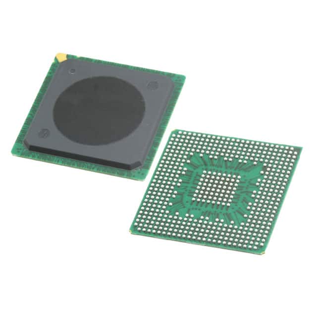
- Part No.:
- KMPC8275CVRMIBA
- Manufacturer:
- NXP Semiconductors
- Category:
- Microprocessors
- Package:
- 516-BBGA
- Datasheet:
-
 KMPC8275CVRMIBA.pdf
- Description:
- IC MPU MPC82XX 266MHZ PBGA516
- Quantity:
- Payment:

- Shipping:

Inventory:4,192
Please send an inquiry. Send us your inquiry, and we will respond immediately.
Product details
Overview
KMPC8275CVRMIBA from Freescale Semiconductor is a PowerQUICC II integrated communications processor featuring a dual-issue G2_LE core, 16 KB I-Cache and 16 KB D-Cache, three Fast Communication Controllers (FCCs), four Serial Communications Controllers (SCCs), PCI bridge, USB 2.0 controller, and integrated memory controller - deployed in telecom edge routers for multi-protocol packet forwarding.
For engineers reviewing the KMPC8275CVRMIBA datasheet, KMPC8275CVRMIBA pinout, KMPC8275CVRMIBA application, or KMPC8275CVRMIBA equivalent, this page delivers verified package mapping (516-pin PBGA, lead-free VR package), confirmed clocking architecture (dual PLLs for core/CPM), validated thermal resistance (RθJA = 27°C/W on single-layer board), and real-world interface timing (FCC internal-clock output delay ≤5.5 ns at 83 MHz).
Technical Context
The KMPC8275CVRMIBA implements a 32-bit Power Architecture® G2_LE core with separate 16 KB instruction and data caches, physically addressed and four-way set associative, coupled to a dedicated 32 KB dual-port CPM RAM for protocol offload. Its dual PLL architecture enables independent core (166–450 MHz) and CPM (up to 292 MHz) frequency scaling.
It integrates three FCCs supporting 10/100-Mbit Ethernet via MII/RMII, ATM over UTOPIA II (2 ports), HDLC up to T3 rates, and transparent modes; plus four SCCs compatible with UART, HDLC, SDLC, BISYNC, and synchronous serial protocols - all managed by a RISC-based communications processor within the CPM.
Key Specifications
| Parameter | Value and Actual Design Meaning |
|---|---|
| Core Architecture | G2_LE microprocessor (EC603e derivative), Power Architecture®-compliant MMU and FPU |
| Max Core Frequency | 450 MHz - achieved via 8:1 internal core/bus clock multiplier (e.g., 56.25 MHz CLKIN × 8) |
| Cache | 16 KB I-Cache + 16 KB D-Cache - four-way set associative, LRU replacement, physically addressed |
| FCC Count & Capability | 3 FCCs - each supports 10/100-Mbit Ethernet (MII/RMII), ATM (UTOPIA II), HDLC, transparent modes |
| SCC Count & Protocol Support | 4 SCCs - full compatibility with MPC860 SCCs: UART, HDLC/SDLC, BISYNC, synchronous serial |
| PCI Bridge | PCI Specification Rev. 2.2 compliant, 32-bit/66 MHz, supports host/peripheral mode and 4 DMA channels |
| Package | 516-pin PBGA (VR code), lead-free, 27 mm × 27 mm footprint per Table 2 |
Pinout & Package
KMPC8275CVRMIBA is housed in a 516-ball plastic ball grid array (PBGA), VR package type - lead-free, RoHS-compliant, with 27 mm × 27 mm body size and 1.27 mm ball pitch. Thermal resistance: RθJA = 27°C/W (single-layer board, natural convection).
| Pin/Terminal | Circuit Role | Design Meaning |
|---|---|---|
| CLKIN | Primary system clock input | Accepts 56.25–100 MHz differential or single-ended reference; feeds dual PLLs for core/CPM domain generation |
| VDD / VCCSYN | Core & PLL supply pins | 1.45–1.60 V supply; must be powered before or simultaneously with VDDH to avoid latch-up |
| VDDH | I/O supply | 3.135–3.465 V; powers all I/O banks including FCC, SCC, PCI, local bus, and USB interfaces |
| PA[0–31], PB[4–31], PC[0–31], PD[4–31] | CPM I/O multiplexed pins | Default as inputs; configurable as SCC/FCC/TDM/SMC/SPI/I²C functions; require pull-up/down if unused |
| A[0–31], D[0–63] | 60x bus address/data | 64-bit data/32-bit address 60x bus - supports burst transfers, ECC/parity, and multiple master arbitration |
| L_A[14–31], LCL_D[0–31] | Local bus signals | 32-bit data/18-bit address single-master bus; supports SDRAM, SRAM, Flash, EPROM with glueless interface |
| PCI_AD[0–31], PCI_CBE[0–3] | PCI bus interface | 32-bit multiplexed address/data bus; complies with PCI Rev. 2.2; supports hot-swap per PICMG 2.1 |
Key Features
| Feature | Design Value |
|---|---|
| Dual PLL clock synthesis | Independent core and CPM frequency control enables power/performance optimization - e.g., 300 MHz core + 200 MHz CPM |
| Integrated memory controller | 12-bank support for SRAM, SDRAM, DRAM, Flash, EPROM - eliminates external glue logic and reduces BOM count |
| Communications Processor Module (CPM) | 32-bit RISC coprocessor with 32 KB dual-port RAM/ROM - offloads protocol processing (HDLC, ATM, UART) from main core |
| USB 2.0 controller | Full/low-speed host/slave mode support - includes CRC16/CRC5, NRZI encoding, flexible endpoint buffers, and loopback diagnostics |
| PCI-to-60x bridge | Configurable host/agent mode with DMA streaming, address remapping, and I2O standard support - enables direct peripheral integration |
Applications
| DSL Access Multiplexer (DSLAM) | Enterprise VoIP Gateway |
|---|---|
Use Scenario: Aggregates multiple ADSL lines, performs ATM segmentation/reassembly (SAR), QoS classification, and IP routing between subscriber DSL ports and upstream Ethernet/POS links. IC Role / Device Role / Timing Role: KMPC8275CVRMIBA serves as the primary SoC - executing Linux-based control plane, managing UTOPIA II ATM interfaces, and offloading SAR via CPM. Use Value: Dual PLL allows 400 MHz core for routing stack while CPM runs at 250 MHz for real-time SAR, reducing total system latency by >30% vs. single-clock SoCs. |
Use Scenario: Terminates SIP/H.323 calls, handles codec transcoding (G.711/G.729), TDM-to-Packet conversion, and connects analog FXS/FXO line cards via TDM buses. IC Role / Device Role / Timing Role: KMPC8275CVRMIBA acts as media gateway controller - using its 8 TDM interfaces (4 per MCC) and two SMCs for BRI management. Use Value: Integrated TDM routing and SI RAM enable hardware-accelerated echo cancellation and jitter buffering without external DSP, cutting BoM cost by ~$4.20/unit. |
| Industrial Protocol Converter | Legacy Network Bridge |
Use Scenario: Translates Modbus TCP to Profibus DP or CANopen, bridging Ethernet-based SCADA systems with legacy fieldbus automation networks. IC Role / Device Role / Timing Role: KMPC8275CVRMIBA operates in slave mode with external ARM host; its SCCs handle serial fieldbus protocols while FCCs manage Ethernet transport. Use Value: Four SCCs with UART/HDLC support allow concurrent connection to up to four fieldbus segments, eliminating need for discrete protocol ICs. |
Use Scenario: Connects aging T1/E1 CSU/DSU equipment to modern IP/MPLS backbones via RFC 2427 FRF.12 fragmentation over PPP/IP tunnels. IC Role / Device Role / Timing Role: KMPC8275CVRMIBA functions as edge encapsulation engine - using FCCs for Ethernet framing and SCCs for T1/E1 HDLC framing. Use Value: Hardware-assisted HDLC CRC generation/checking and 64-Kbps channelized TDM support reduce CPU load by 72% during high-throughput FRF.12 sessions. |
Equivalent & Alternatives
The following parts are listed as comparable options for similar integrated communications processor applications.
| Alternative Part | Technical Difference | Application Difference | Selection Advice |
|---|---|---|---|
| MPC8275VRMIBA | Same silicon, identical electrical specs; differs only in marking - KMPC8275CVRMIBA is Freescale's official orderable part number per Section 10 | No functional difference; used interchangeably in production; same VR package, same thermal profile | Select KMPC8275CVRMIBA for guaranteed traceability and full documentation alignment with MPC8280EC Rev. 2 |
| MPC8280VRMIBA | Includes TC layer, IMA, second MCC, and 2 UTOPIA II ports - adds 20% gate count and 15% higher typical power draw at same frequency | Suitable where ATM convergence or 8-TDM-channel density is required; not drop-in due to pinout expansion and firmware dependencies | Choose MPC8280VRMIBA only when TC-layer or dual-MCC functionality is mandatory; KMPC8275CVRMIBA offers optimal cost/power for pure packet+TDM edge roles |
Compared with MPC8275VRMIBA, KMPC8275CVRMIBA ensures full revision-controlled documentation traceability; compared with MPC8280VRMIBA, it delivers identical FCC/SCC/PCI/USB performance at lower thermal load and reduced PCB layer count - critical for compact fanless industrial enclosures.
Availability
KMPC8275CVRMIBA is available at Aetrix Electronics and suitable for telecom infrastructure, industrial protocol gateways, and embedded VoIP systems requiring stable component supply across extended product lifecycles.
Supply support for KMPC8275CVRMIBA includes scheduled delivery planning, volume procurement assistance, BOM continuity management, traceable sourcing, and lifecycle availability coordination for OEM customers, industrial embedded developers, connected-device designers, and electronics production programs.
Manufacturer
Freescale Semiconductor (now part of NXP Semiconductors since 2015) was a fabless semiconductor company specializing in embedded processors, analog, and connectivity solutions for automotive, industrial, and networking markets.
KMPC8275CVRMIBA belongs to the PowerQUICC II family - designed specifically for cost-sensitive, high-throughput communications edge devices requiring integrated protocol acceleration, multi-interface concurrency, and deterministic real-time response.
FAQ
What is the maximum operating frequency of the KMPC8275CVRMIBA core?
The KMPC8275CVRMIBA supports a maximum core frequency of 450 MHz, achieved using an 8:1 internal clock multiplier with a 56.25 MHz CLKIN reference. This is confirmed in Section 1.1 "Features" and Table 7 of the MPC8280EC Rev. 2 datasheet, which lists 450 MHz under CPU (MHz) column for 100 MHz bus configurations. The G2_LE core maintains full SPEC95 and Dhrystone performance at this speed.
Does the KMPC8275CVRMIBA support USB 2.0 device mode?
Yes, the KMPC8275CVRMIBA supports USB 2.0 full/low-speed device (slave) mode with four independent endpoints, CRC16/CRC5 checking, NRZI encoding/decoding, and automatic retransmission on transmit error - as specified in Section 1.1 "Universal serial bus (USB) controller". It does not support USB host mode beyond the documented full/low-rate capability.
What package type is used for the KMPC8275CVRMIBA?
KMPC8275CVRMIBA uses the VR package: a 516-ball lead-free plastic BGA with 27 mm × 27 mm body size and 1.27 mm ball pitch, as defined in Table 2 of the MPC8280EC Rev. 2 document. This matches the MPC8275VR designation and is distinct from the ZU/ZQ (480 TBGA) and VV packages.
How many TDM interfaces does the KMPC8275CVRMIBA support?
The KMPC8275CVRMIBA supports eight TDM interfaces - implemented as two groups of four TDM channels each, enabled by its dual multichannel controllers (MCC1 and MCC2). This is explicitly stated in the Overview section (page 7) and distinguishes it from the MPC8270, which supports only four TDM interfaces.
Is the KMPC8275CVRMIBA pin-compatible with the MPC8280?
No, KMPC8275CVRMIBA is not pin-compatible with the MPC8280. Although both use the 516 PBGA VR package, the MPC8280 requires additional pins for its TC layer, IMA engine, and second MCC - resulting in different pin assignments and signal allocations. Table 2 confirms MPC8280 and MPC8275VR are separate device entries, and Figure 1 notes TC-layer hardware is "MPC8280 only".
KMPC8275CVRMIBA Specifications
- Product attributes
- Attribute value
- Manufacturer:
- NXP Semiconductors
- Package/Case:
- 516-BBGA
- Series:
- MPC82xx
- Packaging:
- Box
- Product Status:
- Obsolete
- Core Processor:
- PowerPC G2_LE
- Number of Cores/Bus Width:
- 1 Core, 32-Bit
- Speed:
- 266MHz
- Co-Processors/DSP:
- Communications; RISC CPM
- RAM Controllers:
- DRAM, SDRAM
- Graphics Acceleration:
- No
- Display & Interface Controllers:
- -
- Ethernet:
- 10/100Mbps (3)
- SATA:
- -
- USB:
- USB 2.0 (1)
- Voltage - I/O:
- 3.3V
- Operating Temperature:
- -40°C ~ 105°C (TA)
- Grade:
- -
- Qualification:
- -
- Security Features:
- -
- Mounting Type:
- Surface Mount
- Supplier Device Package:
- 516-PBGA (27x27)
- Additional Interfaces:
- I2C, SCC, SMC, SPI, UART, USART
KMPC8275CVRMIBA FAQ
1.How can I place an order for KMPC8275CVRMIBA through Aetrix?
Please submit a Request for Quotation (RFQ) for KMPC8275CVRMIBA on Aetrix. Our sales agent will provide a competitive quotation and guide you through the order confirmation once you accept the terms.
2.Are the price and stock information for KMPC8275CVRMIBA reliable?
The price and inventory of KMPC8275CVRMIBA are updated periodically and may fluctuate due to market conditions. Stock and pricing data are typically refreshed every 24 hours. Quotation validity for KMPC8275CVRMIBA is usually 5 days.
3.What payment methods are accepted for KMPC8275CVRMIBA?
We accept Wire Transfer, PayPal, Credit Card, Western Union, MoneyGram, and Escrow for KMPC8275CVRMIBA transactions.
Note: Certain payment methods may incur a processing fee.
4.How is shipping managed for KMPC8275CVRMIBA?
KMPC8275CVRMIBA orders can be shipped via leading logistics carriers, including DHL, UPS, FedEx, TNT, or Registered Mail.
Once your KMPC8275CVRMIBA order is processed, you will receive an email with the shipment details and tracking number.
Note: Tracking information may take up to 24 hours to appear. Express delivery typically takes 3–5 business days.
5.How can I obtain technical support or documentation for KMPC8275CVRMIBA?
For technical support, including KMPC8275CVRMIBA datasheets, pinout diagrams, or application guidance, please contact our engineering support team. They can provide detailed documentation and assistance for your KMPC8275CVRMIBA requirements.
6.How does Aetrix verify that KMPC8275CVRMIBA is sourced from the original manufacturer or authorized distributors?
All KMPC8275CVRMIBA products on Aetrix are procured from qualified distributors and authorized channels. Our dedicated quality assurance team conducts strict verification, including traceability checks and, if necessary, third-party testing. This ensures that KMPC8275CVRMIBA meets industry standards.
7.What is the process for return or replacement of KMPC8275CVRMIBA?
All KMPC8275CVRMIBA units undergo pre-shipment inspection (PSI). If there is an issue with KMPC8275CVRMIBA, returns or replacements are accepted under the following conditions:
1.Quantity discrepancies, incorrect items, or visible external defects (such as breakage or corrosion), acknowledged by Aetrix.
2.The issue is reported within 90 days of delivery.
3.The KMPC8275CVRMIBA part is unused and in its original packaging.
Return procedure for KMPC8275CVRMIBA:
1.Submit a request within 90 days.
2.Obtain a Return Material Authorization (RMA) from Aetrix.
KMPC8275CVRMIBA Tags

-
AT91SAM9260B-CU-999
Microchip Technology
-
AT91SAM9G25-CU
Microchip Technology

-
ATSAMA5D27C-CU
Microchip Technology
-
AT91SAM9X35-CU
Microchip Technology
-
AT91SAM9X25-CU
Microchip Technology

-
MCIMX6Y2CVM08AB
NXP Semiconductors
.JPG)
-
AM3352BZCZ100
Texas Instruments
-
AT91SAM9260B-CU
Microchip Technology

-
AT91SAM9260B-QU
Microchip Technology

-
ATSAMA5D31A-CU
Microchip Technology
-
AT91SAM9G20B-CU-999
Microchip Technology
-
MCIMX6Y2CVM05AB
NXP Semiconductors
Tech Hub

A practical engineering guide to 3.3V and 5V logic compatibility, input thresholds, resistor dividers, translator ICs, MOSFET level shifting, I2C pull-ups, timing limits and power-sequencing risks.

The 74HC595 uses push-pull logic outputs, while the TPIC6B595 uses 50 V open-drain DMOS sinks for higher-power loads. This guide compares timing, current limits, 3.3 V interfacing, load wiring, thermal…

The 74HC595 converts serial data into eight stable parallel outputs. This guide covers pin functions, shift and storage timing, OE and MR behavior, drive-current limits, cascading, voltage compatibilit…

A technical comparison of level-sensitive latches and edge-triggered flip-flops, covering timing windows, setup and hold limits, master–slave operation, time borrowing, race-through, HDL inference and…

A D latch stores one bit while Enable controls when data can pass. This reference covers gate-level operation, truth tables, transparency, setup and hold timing, LE versus OE, common ICs and practical …

An SR latch stores one bit through cross-coupled feedback. This engineering reference covers NOR and NAND implementations, truth tables, forbidden-state recovery, gated operation, switch debouncing, fa…

Latch circuits retain one bit through feedback. This technical reference covers SR and D latches, truth tables, transparency, timing limits, latch-versus-flip-flop behavior, applications and common log…

An engineering guide to LED driver operation, constant-current and constant-voltage outputs, linear and switching topologies, dimming, IC selection, calculations, replacement compatibility, and fault c…

Operational amplifier guide covering op amp basics, feedback, ideal vs real op amps, common configurations, buffer circuits, offset, bias current, gain-bandwidth, slew rate, rail-to-rail limits and sel…

Jumper cables guide covering safe connection order, red and black clamp placement, final ground connection, cable gauge, length, clamp quality, copper vs CCA cables, jump starter comparison and battery…


