
 My Inquiry
 My Account


onsemi KSC3503DSTSTU
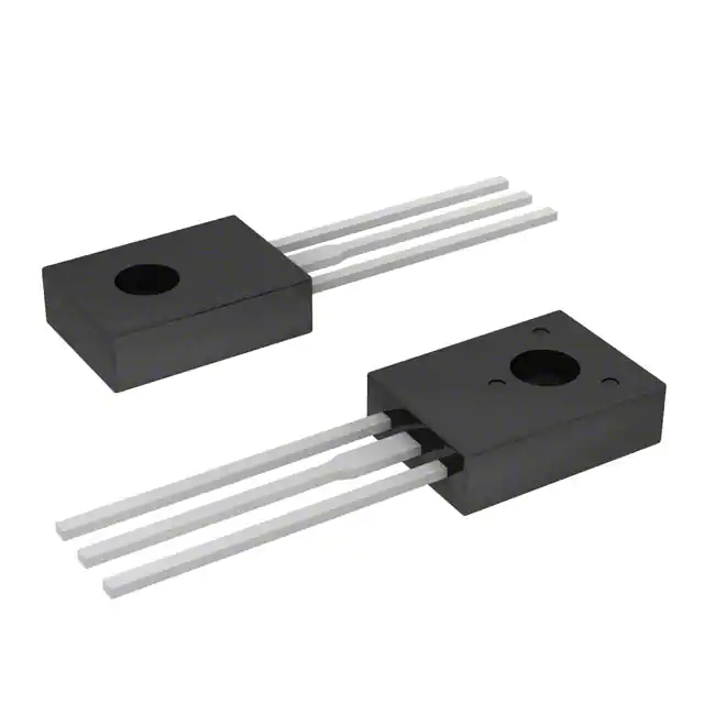
- Part No.:
- KSC3503DSTSTU
- Manufacturer:
- onsemi
- Category:
- Single Bipolar Transistors
- Package:
- TO-225AA, TO-126-3
- Datasheet:
-
 KSC3503DSTSTU.pdf
- Description:
- TRANS NPN 300V 0.1A TO-126-3
- Quantity:
- Payment:

- Shipping:

Inventory:9,083
Please send an inquiry. Send us your inquiry, and we will respond immediately.
Product details
Overview
KSC3503DSTU from onsemi is an NPN epitaxial silicon transistor designed for high-voltage audio and video amplifier stages, featuring VCEO = 300 V, fT = 150 MHz, hFE = 60–120 (at IC = 10 mA), Cob = 1.8–2.6 pF, and TO-126-3LD package. It serves as a voltage/current amplifier in CRT display output and low-THD audio circuits.
For engineers reviewing the KSC3503DSTU datasheet, pinout, applications, or equivalent options, key selection criteria include high-voltage breakdown rating, gain linearity at audio frequencies, thermal resistance (RθJC = 17.8°C/W), and Pb-free RoHS-compliant packaging for legacy CRT and analog video systems.
Technical Context
This device operates as a medium-power NPN bipolar junction transistor optimized for linear amplification in analog signal paths. Its 300 V collector-emitter and collector-base breakdown ratings enable use in high-swing video output stages, while its 150 MHz fT supports wideband audio and baseband video bandwidths without phase distortion.
The low reverse transfer capacitance (Cre = 1.8 pF at VCB = 30 V) and excellent hFE linearity across IC = 1–100 mA reduce harmonic distortion in Class-A and AB amplifier configurations. Thermal design is supported by full SPICE models and RθJC = 17.8°C/W for mounting on heatsinks.
Key Specifications
| Parameter | Value and Actual Design Meaning |
|---|---|
| VCEO | 300 V - Enables safe operation in CRT anode drive and high-voltage audio supply rails. |
| fT | 150 MHz - Supports full NTSC/PAL video bandwidth and extended audio frequency response up to 20 kHz with margin. |
| hFE | 60–120 @ IC = 10 mA - Provides stable DC biasing and predictable small-signal gain in emitter-follower and common-emitter topologies. |
| Cob | 1.8–2.6 pF @ VCB = 30 V - Minimizes Miller effect in high-gain amplifier stages, preserving stability and slew rate. |
| RθJC | 17.8°C/W - Allows direct mounting to heatsink for continuous 7 W dissipation at TC = 25°C without derating. |
| VBE(sat) | 1.0 V @ IC = 20 mA, IB = 2 mA - Ensures reliable saturation in current-source and switching-auxiliary roles within analog subsystems. |
Pinout & Package
Package: TO-126-3LD (Case 340AS), surface-mount compatible through-hole package with integral metal tab for heatsinking. Mounting pad minimizes thermal resistance to heatsink.
| Pin/Terminal | Circuit Role | Design Meaning |
|---|---|---|
| 1 (Emitter) | Current sink terminal | Low-impedance return path; connects to ground or negative rail in common-emitter configuration. |
| 2 (Collector) | Current source terminal | High-voltage output node; directly drives CRT deflection yoke or video load impedance. |
| 3 (Base) | Control input | Receives bias current to set operating point; requires external resistor network for stable Q-point. |
Key Features
| Feature | Design Value |
|---|---|
| High-voltage capability | VCEO = VCBO = 300 V enables direct integration into CRT horizontal output and flyback transformer driver circuits. |
| Low reverse transfer capacitance | Cre = 1.8 pF reduces feedback coupling in high-gain amplifiers, improving stability and reducing THD in audio applications. |
| Gain linearity | hFE variation < ±15% over IC = 1–50 mA ensures consistent amplification across dynamic signal range in voltage amplifier stages. |
| Pb-free & RoHS compliant | Meets EU Directive 2011/65/EU; suitable for industrial repair and legacy system replacement where leaded parts are restricted. |
Applications
| Audio Voltage Amplifier | Video Output Stage |
|---|---|
Use Scenario: Low-distortion preamplifier and line driver in analog audio equipment. IC Role / Device Role / Timing Role: NPN voltage amplifier in common-emitter configuration with emitter degeneration. Use Value: hFE linearity and low Cob maintain THD < 0.05% at 1 kHz, supporting Hi-Fi signal integrity. | Use Scenario: CRT monitor video output buffer driving 75 Ω coaxial cable. IC Role / Device Role / Timing Role: Emitter-follower current booster for composite video signal. Use Value: 300 V VCEO withstands sync pulse overshoot; 150 MHz fT preserves rise/fall times < 2.3 ns. |
| CRT Horizontal Deflection | Analog Current Source |
Use Scenario: Horizontal output transistor in CRT TV flyback circuitry. IC Role / Device Role / Timing Role: Switching transistor in self-oscillating horizontal deflection stage. Use Value: 300 V breakdown rating accommodates flyback voltage spikes; RθJC = 17.8°C/W enables heatsink mounting for 7 W peak dissipation. | Use Scenario: Constant-current source for LED biasing or sensor excitation in industrial analog modules. IC Role / Device Role / Timing Role: Active current regulator using emitter resistor feedback. Use Value: Stable hFE and low ICBO (< 0.1 μA) ensure < 2% current drift over −40°C to +125°C ambient. |
Equivalent & Alternatives
The following parts are listed as comparable options for similar NPN high-voltage amplifier applications.
| Alternative Part | Technical Difference | Application Difference | Selection Advice |
|---|---|---|---|
| KSC3502DSTU | VCEO = 200 V (lower), fT = 120 MHz, same TO-126 package and pinout. | Not suitable for 300 V CRT flyback or high-swing video; limited to mid-voltage audio and general-purpose amplification. | Select only if system voltage remains ≤ 200 V and bandwidth requirements are relaxed. |
| 2SC5200 | VCEO = 230 V, IC = 15 A (higher), TO-3P package, no Pb-free option in standard offering. | Designed for high-current audio power output; incompatible pinout and thermal interface; not drop-in. | Consider only for new designs requiring >100 mA continuous current and accepting larger footprint and lead-free compliance trade-off. |
Compared with KSC3503DSTU, KSC3502DSTU offers reduced voltage headroom but identical form factor, while 2SC5200 delivers higher current capability at the cost of package compatibility and RoHS status-making KSC3503DSTU optimal for legacy CRT repair and precision analog voltage amplification where 300 V and low capacitance are mandatory.
Availability
KSC3503DSTU is available at Aetrix Electronics and suitable for CRT display repair, analog audio amplifier refurbishment, and industrial video signal conditioning requiring stable component supply and long-lifecycle support.
Supply support for KSC3503DSTU includes scheduled delivery planning, volume procurement assistance, BOM continuity management, traceable sourcing, and lifecycle availability coordination for OEM customers, industrial embedded developers, connected-device designers, and electronics production programs.
Manufacturer
onsemi (formerly ON Semiconductor) is a global semiconductor supplier specializing in energy-efficient power, analog, sensing, and connectivity solutions for automotive, industrial, cloud, and consumer markets.
The KSC3503DSTU belongs to onsemi's high-voltage discrete transistor product line, engineered specifically for analog video, CRT deflection, and low-THD audio amplifier applications demanding reliability under sustained high-voltage stress.
FAQ
What is the maximum collector-emitter voltage rating for KSC3503DSTU?
The KSC3503DSTU has a guaranteed minimum collector-emitter breakdown voltage (BVCEO) of 300 V at IC = 1 mA and IB = 0. This rating is validated per onsemi's absolute maximum ratings table and applies under DC conditions at TA = 25°C. Derating is required above 25°C ambient per the power derating curve in Figure 10 of the datasheet. The KSC3503DSTU must not be operated beyond this limit to prevent irreversible junction failure.
Is KSC3503DSTU RoHS compliant and lead-free?
Yes, the KSC3503DSTU is explicitly marked Pb-free and RoHS compliant per onsemi's datasheet revision 3 (April 2025). The "DS" suffix denotes the Pb-free version in TO-126-3LD packaging, and the marking "C3503D" on the device body confirms compliance. This makes KSC3503DSTU suitable for repair and manufacturing in regions enforcing EU Directive 2011/65/EU, including industrial and broadcast equipment servicing.
What is the thermal resistance from junction to case for KSC3503DSTU?
The thermal resistance from junction to case (RθJC) for KSC3503DSTU is 17.8°C/W when mounted on minimum pad size, as specified in the Thermal Characteristics table. This value assumes proper mechanical contact between the TO-126 metal tab and an external heatsink. For continuous operation at 7 W, case temperature must remain ≤ 25°C; above that, power must be linearly derated per Figure 10. The KSC3503DSTU's RθJC enables efficient heat extraction in space-constrained CRT and amplifier chassis.
Does KSC3503DSTU have SPICE models available for simulation?
Yes, onsemi provides full thermal and electrical SPICE models for the KSC3503DSTU, as stated in the Features section of the official datasheet. These models include accurate junction temperature behavior, nonlinear capacitance, and gain compression effects. Engineers can download them directly from onsemi's website under the KSC3503 product page in the Technical Documentation section. Using these models ensures realistic simulation of KSC3503DSTU performance in audio amplifier and video output circuit designs.
What is the typical output capacitance (Cob) of KSC3503DSTU and how does it affect circuit stability?
The KSC3503DSTU exhibits Cob = 1.8 pF (typical) and 2.6 pF (max) at VCB = 30 V and f = 1 MHz. This low output capacitance minimizes Miller multiplication in common-emitter amplifiers, preserving phase margin and preventing oscillation at high frequencies. In video output stages, it maintains signal fidelity by limiting high-frequency roll-off. The KSC3503DSTU's Cob is significantly lower than general-purpose transistors, making it especially valuable in wideband analog designs where stability and bandwidth are critical.
KSC3503DSTSTU Specifications
- Product attributes
- Attribute value
- Manufacturer:
- onsemi
- Series:
- -
- Package/Case:
- TO-225AA, TO-126-3
- Packaging:
- Tube
- Product Status:
- Obsolete
- Transistor Type:
- NPN
- Current - Collector (Ic) (Max):
- 100 mA
- Voltage - Collector Emitter Breakdown (Max):
- 300 V
- Vce Saturation (Max) @ Ib, Ic:
- 600mV @ 2mA, 20mA
- Current - Collector Cutoff (Max):
- 100nA (ICBO)
- DC Current Gain (hFE) (Min) @ Ic, Vce:
- 60 @ 10mA, 10V
- Power - Max:
- 7 W
- Frequency - Transition:
- 150MHz
- Operating Temperature:
- -55°C ~ 150°C (TJ)
- Grade:
- -
- Qualification:
- -
- Mounting Type:
- Through Hole
- Supplier Device Package:
- TO-126-3
KSC3503DSTSTU FAQ
1.How can I place an order for KSC3503DSTSTU through Aetrix?
Please submit a Request for Quotation (RFQ) for KSC3503DSTSTU on Aetrix. Our sales agent will provide a competitive quotation and guide you through the order confirmation once you accept the terms.
2.Are the price and stock information for KSC3503DSTSTU reliable?
The price and inventory of KSC3503DSTSTU are updated periodically and may fluctuate due to market conditions. Stock and pricing data are typically refreshed every 24 hours. Quotation validity for KSC3503DSTSTU is usually 5 days.
3.What payment methods are accepted for KSC3503DSTSTU?
We accept Wire Transfer, PayPal, Credit Card, Western Union, MoneyGram, and Escrow for KSC3503DSTSTU transactions.
Note: Certain payment methods may incur a processing fee.
4.How is shipping managed for KSC3503DSTSTU?
KSC3503DSTSTU orders can be shipped via leading logistics carriers, including DHL, UPS, FedEx, TNT, or Registered Mail.
Once your KSC3503DSTSTU order is processed, you will receive an email with the shipment details and tracking number.
Note: Tracking information may take up to 24 hours to appear. Express delivery typically takes 3–5 business days.
5.How can I obtain technical support or documentation for KSC3503DSTSTU?
For technical support, including KSC3503DSTSTU datasheets, pinout diagrams, or application guidance, please contact our engineering support team. They can provide detailed documentation and assistance for your KSC3503DSTSTU requirements.
6.How does Aetrix verify that KSC3503DSTSTU is sourced from the original manufacturer or authorized distributors?
All KSC3503DSTSTU products on Aetrix are procured from qualified distributors and authorized channels. Our dedicated quality assurance team conducts strict verification, including traceability checks and, if necessary, third-party testing. This ensures that KSC3503DSTSTU meets industry standards.
7.What is the process for return or replacement of KSC3503DSTSTU?
All KSC3503DSTSTU units undergo pre-shipment inspection (PSI). If there is an issue with KSC3503DSTSTU, returns or replacements are accepted under the following conditions:
1.Quantity discrepancies, incorrect items, or visible external defects (such as breakage or corrosion), acknowledged by Aetrix.
2.The issue is reported within 90 days of delivery.
3.The KSC3503DSTSTU part is unused and in its original packaging.
Return procedure for KSC3503DSTSTU:
1.Submit a request within 90 days.
2.Obtain a Return Material Authorization (RMA) from Aetrix.
KSC3503DSTSTU Tags
-
MMBT3906LT1G
onsemi
-
MMBT3904-7-F
Diodes Incorporated
-
MMBT3904LT1G
onsemi
-
MMBT3906-7-F
Diodes Incorporated
-
MMBT3904-TP
Micro Commercial Co
-
MMBT2222A-7-F
Diodes Incorporated
-
BC846BLT1G
onsemi
-
BC847B,215
Nexperia USA Inc.
-
SMMBT3904LT1G
onsemi
-
MMBT2222A-TP
Micro Commercial Co
-
MMBTA06LT1G
onsemi
-
MMBT2222ALT1G
onsemi
Tech Hub

Counterfeit components can hide behind convincing markings and passing basic function tests. This engineering reference covers source traceability, external inspection, X-ray, XRF, electrical testing, …

A practical engineering and sourcing framework covering lifecycle verification, lifetime-buy calculations, replacement qualification, supplier checks and counterfeit-risk controls.

TTL and CMOS logic families differ in thresholds, loading, output drive, power and timing. This engineering guide compares 74HC and 74HCT, calculates noise margins and checks 3.3 V/5 V compatibility.

A practical engineering guide to 3.3V and 5V logic compatibility, input thresholds, resistor dividers, translator ICs, MOSFET level shifting, I2C pull-ups, timing limits and power-sequencing risks.

The 74HC595 uses push-pull logic outputs, while the TPIC6B595 uses 50 V open-drain DMOS sinks for higher-power loads. This guide compares timing, current limits, 3.3 V interfacing, load wiring, thermal…

The 74HC595 converts serial data into eight stable parallel outputs. This guide covers pin functions, shift and storage timing, OE and MR behavior, drive-current limits, cascading, voltage compatibilit…

A technical comparison of level-sensitive latches and edge-triggered flip-flops, covering timing windows, setup and hold limits, master–slave operation, time borrowing, race-through, HDL inference and…

A D latch stores one bit while Enable controls when data can pass. This reference covers gate-level operation, truth tables, transparency, setup and hold timing, LE versus OE, common ICs and practical …

An SR latch stores one bit through cross-coupled feedback. This engineering reference covers NOR and NAND implementations, truth tables, forbidden-state recovery, gated operation, switch debouncing, fa…

Latch circuits retain one bit through feedback. This technical reference covers SR and D latches, truth tables, transparency, timing limits, latch-versus-flip-flop behavior, applications and common log…


