
 My Inquiry
 My Account


STMicroelectronics L6728ATR
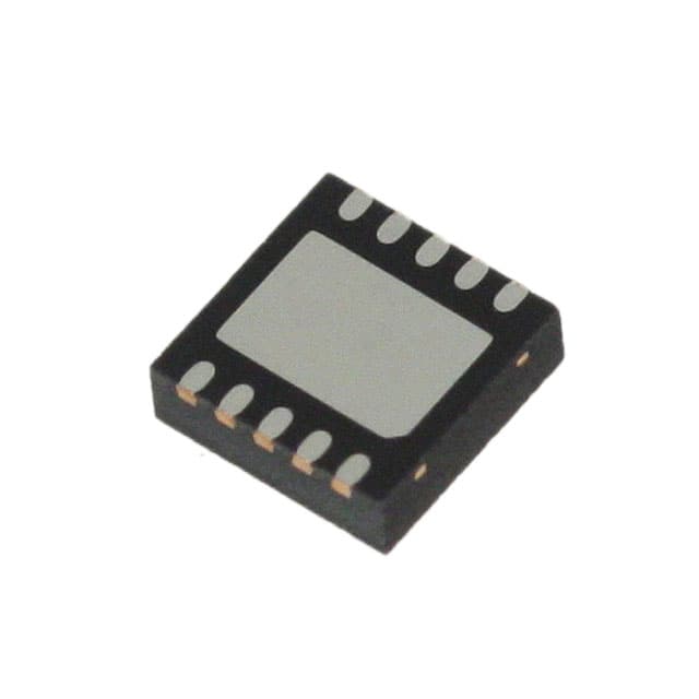
- Part No.:
- L6728ATR
- Manufacturer:
- STMicroelectronics
- Category:
- DC DC Switching Controllers
- Package:
- 10-VFDFN Exposed Pad
- Datasheet:
-
 L6728ATR.pdf
- Description:
- IC REG CTRLR BUCK 10-VFQFPN
- Quantity:
- Payment:

- Shipping:

Inventory:914
Please send an inquiry. Send us your inquiry, and we will respond immediately.
Product details
Overview
L6728ATR from STMicroelectronics is a high-frequency single-phase synchronous buck PWM controller with integrated high-current gate drivers, 0.8 V internal reference, ±0.8 % output voltage accuracy, fixed 600 kHz switching frequency, and sensorless over-current protection via low-side RDS(on) sensing - designed for CPU/DSP and subsystem power supplies requiring fast transient response and pre-bias start-up capability.
For engineers reviewing the L6728ATR datasheet, L6728ATR pinout, L6728ATR application, or L6728ATR equivalent, key selection considerations include its VFDFPN10 package footprint, LS-LESS pre-bias startup behavior, dual-level OCP programmability via ROCSET, and VSEN-based OVP/UVP/PGOOD monitoring independent of FB divider.
Technical Context
L6728ATR implements voltage-mode control with a 15 MHz GBWP error amplifier and 8 V/μs slew rate to support high-bandwidth regulation. Its adaptive anti-cross-conduction logic uses PHASE and LGATE pin sensing to dynamically adjust dead time, minimizing body-diode conduction without external Schottky diodes.
The controller supports input conversion down to 1.5 V while operating from a 5–12 V VCC supply. It enables sensorless current sensing by comparing PHASE node voltage during LS conduction against user-programmed (via ROCSET) and internally scaled (×1.5) OCP thresholds, eliminating sense resistors.
Key Specifications
| Parameter | Value and Actual Design Meaning |
|---|---|
| Switching frequency | Fixed 600 kHz - enables compact magnetics and predictable EMI profile without external timing components. |
| Output voltage accuracy | ±0.8 % over line/load/temperature - ensures tight regulation for sensitive digital loads like CPUs and memory I/O. |
| Reference voltage | 0.8 V internal - allows direct regulation of 0.8 V outputs; higher voltages set via FB resistor divider. |
| Gate drive capability | HS: 1.5 A source / 1.1 Ω sink; LS: 1.5 A source / 0.65 Ω sink - drives multiple parallel MOSFETs in high-current buck stages. |
| OCP threshold range | Programmable 50–550 mV via ROCSET - maps directly to sensed RDS(on) drop, enabling precise current limiting without sense resistors. |
| PGOOD window | VSEN upper: 0.890 V, lower: 0.710 V - provides robust power-good signaling with hysteresis for stable system sequencing. |
| Soft-start duration | 4.5 ms typical - linearly ramps internal reference to limit inrush current into output capacitors. |
Pinout & Package
Supplied in VFDFPN10 (3 × 3 mm, 0.5 mm pitch) with exposed thermal pad - optimized for high-power density DC-DC converters requiring efficient heat dissipation in space-constrained applications.
| Pin/Terminal | Circuit Role | Design Meaning |
|---|---|---|
| 1 BOOT | HS driver bootstrap supply | Connects via 100 nF capacitor to PHASE node; supplies floating gate drive for high-side N-MOSFET. |
| 2 PHASE | HS return / current sense node | Monitors LS RDS(on) voltage drop for OCP; also used for adaptive dead-time detection and LS-less startup logic. |
| 3 UGATE | High-side gate driver output | Direct drive output for HS MOSFET gate; capable of 1.5 A peak source/sink current. |
| 4 LGATE / OC | Low-side gate driver output & OCP programming | Drives LS MOSFET gate; sources 10 µA during startup to set OCP threshold via ROCSET resistor to GND. |
| 5 GND | Power and signal reference | Common return for all internal circuits, drivers, and protections; must connect to low-impedance PCB ground plane. |
| 6 VCC | Controller and driver supply | Operates from 5–12 V; powers internal logic and LS driver; requires ≥1 µF MLCC decoupling to GND. |
| 7 COMP / DIS | Error amplifier output & disable input | Compensation node for EA loop; pulled <0.75 V to disable controller; open for normal operation. |
| 8 FB | Error amplifier inverting input | Connects to output voltage divider; compares regulated output against 0.8 V reference for closed-loop control. |
| 9 VSEN | Output voltage monitor | Dedicated pin for OVP/UVP/PGOOD; senses actual output (or divider tap) independently of FB path for robust protection. |
| 10 PGOOD | Open-drain power-good indicator | Pulled low when VSEN is outside 0.71–0.89 V window; requires external pull-up ≤ VCC for system sequencing. |
Key Features
| Feature | Design Value |
|---|---|
| LS-LESS pre-bias startup | Enables safe soft-start into pre-charged outputs by delaying LS turn-on until HS switching begins - prevents negative voltage spikes and inductor current reversal. |
| Sensorless dual-level OCP | First-level OCP triggered after four consecutive cycles exceeding ROCSET-set threshold; second-level OCP triggers immediately at 1.5× threshold - balances fault tolerance and safety. |
| VSEN-based protection independence | OVP, UVP, and PGOOD functions operate on dedicated VSEN pin, decoupled from FB divider network - eliminates false trips due to divider resistor drift or disconnection. |
| Adaptive dead-time control | Uses real-time PHASE and LGATE voltage monitoring to minimize shoot-through and body-diode conduction - improves efficiency without external timing components. |
| Integrated high-current drivers | HS and LS drivers each deliver 1.5 A peak current with low on-resistance (1.1 Ω HS sink, 0.65 Ω LS sink) - supports high-efficiency synchronous rectification with discrete MOSFETs. |
Applications
| Memory and Termination Supply | CPU and DSP Power Supply |
|---|---|
|
Use Scenario: Providing tightly regulated 1.2 V or 1.5 V to DDR memory modules and bus termination networks in servers and workstations. IC Role / Device Role / Timing Role: Primary synchronous buck controller managing dynamic load transients during burst data transfers and clock-gated idle states. Use Value: ±0.8 % voltage accuracy and 600 kHz switching ensure stable memory interface timing margins; LS-LESS prevents corruption during hot-plug or warm-reset events. |
Use Scenario: Delivering scalable core voltage (e.g., 0.8–1.3 V) to modern x86 or ARM processors with dynamic voltage/frequency scaling (DVFS). IC Role / Device Role / Timing Role: Voltage-mode PWM controller coordinating with VRM-compatible VID interface (via external DAC/resistor network) for precise VOUT adjustment. Use Value: 15 MHz GBWP and 8 V/μs slew rate enable sub-10 μs transient recovery; VSEN monitoring guarantees reliable PGOOD assertion before processor release from reset. |
| Subsystem Power Supply (MCH/IOCH) | Distributed Power Supply |
|
Use Scenario: Generating isolated 3.3 V or 5 V rails for memory controller hubs (MCH), I/O controller hubs (IOCH), and PCI Express switch logic. IC Role / Device Role / Timing Role: Standalone step-down controller powering secondary logic domains with independent sequencing and fault isolation. Use Value: Dual-level OCP protects against short-circuited daughterboards; UVLO hysteresis (4.1 V ON, 3.9 V OFF) prevents brownout oscillation during rail collapse. |
Use Scenario: Local point-of-load (POL) conversion in telecom line cards, industrial PLCs, or automotive domain controllers where centralized 12 V bus feeds multiple distributed loads. IC Role / Device Role / Timing Role: Compact, thermally efficient buck controller mounted near load to minimize IR drop and EMI radiation. Use Value: VFDFPN10 package with exposed pad enables >2 W dissipation in 9 mm² area; 45 °C/W θJA supports operation up to 125 °C junction temperature. |
Equivalent & Alternatives
The following parts are listed as comparable options for similar synchronous buck controller applications.
| Alternative Part | Technical Difference | Application Difference | Selection Advice |
|---|---|---|---|
| ISL6269CRZ-T | Fixed 500 kHz frequency; requires external bootstrap diode; no LS-LESS feature; OCP via sense resistor only. | Lacks pre-bias startup and sensorless current sensing - unsuitable for hot-plug memory or cost-sensitive designs avoiding sense resistors. | Select if legacy design uses sense resistors and prioritizes mature qualification over integration. |
| TPS54620RGYR | Integrated FETs (30 V, 6 A); 2.95–17 V input; adjustable 300–2000 kHz; no VSEN pin - protections tied to FB. | Monolithic solution eliminates external MOSFET layout complexity but limits max output current and thermal headroom vs. controller+discrete approach. | Select for lower BOM count and simplified layout where 6 A output and 17 V input suffice. |
Compared with ISL6269CRZ-T and TPS54620RGYR, L6728ATR uniquely combines sensorless OCP, LS-LESS startup, and VSEN-decoupled protections in a 10-pin VFDFPN - offering superior flexibility for high-reliability, high-density POL designs where discrete MOSFET optimization and robust sequencing are critical.
Availability
L6728ATR is available at Aetrix Electronics and suitable for CPU and DSP power supply, memory termination, subsystem power (MCH/IOCH), and distributed POL applications requiring stable component supply, long-lifecycle support, and consistent parametric performance across production batches.
Supply support for L6728ATR includes scheduled delivery planning, volume procurement assistance, BOM continuity management, traceable sourcing, and lifecycle availability coordination for OEM customers, industrial embedded developers, connected-device designers, and electronics production programs.
Manufacturer
STMicroelectronics is a global semiconductor leader headquartered in Geneva, specializing in power management, microcontrollers, and analog ICs for industrial, automotive, and consumer markets.
L6728ATR belongs to ST's high-frequency PWM controller product line, engineered specifically for high-efficiency, space-constrained synchronous buck converters in computing and communications infrastructure where precision regulation and robust fault handling are mandatory.
FAQ
What is the purpose of the VSEN pin, and how does it differ from the FB pin?
VSEN is a dedicated output voltage monitor pin used exclusively for over-voltage, under-voltage, and PGOOD protection functions. Unlike FB - which feeds the error amplifier for regulation - VSEN operates independently, allowing accurate protection even if the FB resistor divider fails or disconnects. It must be connected directly to the output or to the same node as the FB divider's top resistor to ensure coordinated regulation and protection thresholds.
How does LS-LESS startup prevent negative voltage spikes during pre-biased output conditions?
During LS-LESS startup, the low-side MOSFET remains disabled until the high-side MOSFET begins switching. This prevents reverse current flow through the inductor when the output is already charged above the target voltage. If the output remains pre-biased after soft-start completes, the LS MOSFET is then enabled to discharge the output safely to the regulated level - avoiding dangerous undershoot and load damage.
Can the L6728ATR operate with an input voltage below 5 V, and what are the limitations?
Yes - the power conversion input can be as low as 1.5 V, but the VCC supply must remain within 5–12 V. The controller itself is powered from VCC, not VIN. Therefore, a separate 5–12 V bias supply (e.g., auxiliary rail or LDO) is mandatory. The 1.5 V minimum applies only to the switched input (VIN), enabling use in intermediate bus architectures such as 3.3 V or 5 V input-to-core-voltage conversion.
What happens when over-current protection is triggered, and how is recovery performed?
Upon detection of a second-level OCP event (exceeding 1.5× programmed threshold), or four consecutive first-level OCP events, the controller latches both UGATE and LGATE low and halts switching. Recovery requires cycling the VCC supply - i.e., removing and reapplying the 5–12 V bias voltage - to reset internal protection latches and restart soft-start. No automatic retry or hiccup mode is implemented.
L6728ATR Specifications
- Product attributes
- Attribute value
- Manufacturer:
- STMicroelectronics
- Series:
- -
- Package/Case:
- 10-VFDFN Exposed Pad
- Packaging:
- Tape & Reel (TR)
- Product Status:
- Obsolete
- Output Type:
- Transistor Driver
- Function:
- Step-Down
- Output Configuration:
- Positive
- Topology:
- Buck
- Number of Outputs:
- 1
- Output Phases:
- 1
- Voltage - Supply (Vcc/Vdd):
- 5V ~ 12V
- Frequency - Switching:
- 600kHz
- Duty Cycle (Max):
- 67%
- Synchronous Rectifier:
- Yes
- Clock Sync:
- No
- Serial Interfaces:
- -
- Control Features:
- Enable, Phase Control, Power Good
- Operating Temperature:
- -40°C ~ 125°C (TJ)
- Grade:
- -
- Qualification:
- -
- Mounting Type:
- Surface Mount
- Supplier Device Package:
- 10-DFN (3x3)
L6728ATR FAQ
1.How can I place an order for L6728ATR through Aetrix?
Please submit a Request for Quotation (RFQ) for L6728ATR on Aetrix. Our sales agent will provide a competitive quotation and guide you through the order confirmation once you accept the terms.
2.Are the price and stock information for L6728ATR reliable?
The price and inventory of L6728ATR are updated periodically and may fluctuate due to market conditions. Stock and pricing data are typically refreshed every 24 hours. Quotation validity for L6728ATR is usually 5 days.
3.What payment methods are accepted for L6728ATR?
We accept Wire Transfer, PayPal, Credit Card, Western Union, MoneyGram, and Escrow for L6728ATR transactions.
Note: Certain payment methods may incur a processing fee.
4.How is shipping managed for L6728ATR?
L6728ATR orders can be shipped via leading logistics carriers, including DHL, UPS, FedEx, TNT, or Registered Mail.
Once your L6728ATR order is processed, you will receive an email with the shipment details and tracking number.
Note: Tracking information may take up to 24 hours to appear. Express delivery typically takes 3–5 business days.
5.How can I obtain technical support or documentation for L6728ATR?
For technical support, including L6728ATR datasheets, pinout diagrams, or application guidance, please contact our engineering support team. They can provide detailed documentation and assistance for your L6728ATR requirements.
6.How does Aetrix verify that L6728ATR is sourced from the original manufacturer or authorized distributors?
All L6728ATR products on Aetrix are procured from qualified distributors and authorized channels. Our dedicated quality assurance team conducts strict verification, including traceability checks and, if necessary, third-party testing. This ensures that L6728ATR meets industry standards.
7.What is the process for return or replacement of L6728ATR?
All L6728ATR units undergo pre-shipment inspection (PSI). If there is an issue with L6728ATR, returns or replacements are accepted under the following conditions:
1.Quantity discrepancies, incorrect items, or visible external defects (such as breakage or corrosion), acknowledged by Aetrix.
2.The issue is reported within 90 days of delivery.
3.The L6728ATR part is unused and in its original packaging.
Return procedure for L6728ATR:
1.Submit a request within 90 days.
2.Obtain a Return Material Authorization (RMA) from Aetrix.
L6728ATR Tags

-
UCC28C45DR
Texas Instruments
-
UCC28C40DR
Texas Instruments
-
UCC28C43DR
Texas Instruments

-
ZXSC410E6TA
Diodes Incorporated

-
LM3524DMX/NOPB
Texas Instruments

-
LM3489MMX/NOPB
Texas Instruments
-
MIC2102YML-TR
Microchip Technology

-
LM5148RGYR
Texas Instruments
-
TL598CDR
Texas Instruments

-
LM5155DSSR
Texas Instruments

-
LM25085MYX/NOPB
Texas Instruments
-
UCC2813DTR-0
Texas Instruments
Tech Hub

Operational amplifier guide covering op amp basics, feedback, ideal vs real op amps, common configurations, buffer circuits, offset, bias current, gain-bandwidth, slew rate, rail-to-rail limits and sel…

Jumper cables guide covering safe connection order, red and black clamp placement, final ground connection, cable gauge, length, clamp quality, copper vs CCA cables, jump starter comparison and battery…

LDO regulator guide covering low dropout voltage, power dissipation, thermal design, PSRR, output noise, capacitor stability, adjustable LDO circuits, LDO vs buck converter and datasheet selection chec…

Conditional Access Module guide covering CAM meaning, CI/CI+ interface, smart card authorization, DVB security workflow, TV and set-top box compatibility, internal electronics, ESD protection, connecto…

Guide to electronic component obsolescence covering EOL risk, PCN/PDN notices, last-time buy planning, replacement options, form-fit-function validation, counterfeit risk and BOM lifecycle management.

18650 battery guide covering lithium-ion cell basics, 3.6V/3.7V voltage, 4.2V charging, mAh and Wh capacity, protected cells, chargers, BMS, series-parallel packs, holders, welding and sourcing checks.…

Hall effect sensor guide covering working principle, linear and digital sensors, Arduino circuits, current sensing, speed detection, automotive applications, A3144 examples, signal filtering and datash…

Product Change Notification guide for electronic components, covering PCN meaning, PCN vs PDN/EOL, common change types, risk levels, form-fit-function review, engineering validation, BOM control, LTB/L…

A practical guide to blend door actuators, covering HVAC function, symptoms, location, AC and heater issues, reset and calibration, replacement cost, electrical diagnosis, compatibility checks, and rep…

Engineering guide to Raspberry Pi alternatives, covering chip-level differences, Orange Pi, ROCK, Jetson, Banana Pi, NanoPi, Compute Module, Pico, GPIO, camera, HAT compatibility, and replacement risks…


