
 My Inquiry
 My Account


STMicroelectronics L9963T-TR
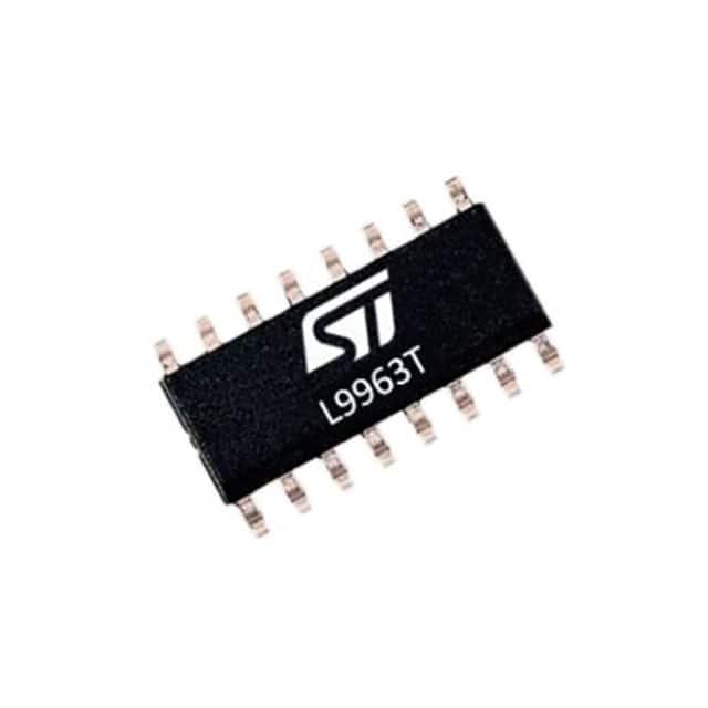
- Part No.:
- L9963T-TR
- Manufacturer:
- STMicroelectronics
- Category:
- Battery Management
- Package:
- 16-SOIC (0.154", 3.90mm Width)
- Datasheet:
-
 L9963T-TR.pdf
- Description:
- AUTOMOTIVE GENERAL PURPOSE SPI T
- Quantity:
- Payment:

- Shipping:

Inventory:1,526
Please send an inquiry. Send us your inquiry, and we will respond immediately.
Product details
Overview
L9963T-TR from STMicroelectronics is an AEC-Q100 qualified, ISO 26262 ASIL-D ready SPI-to-isolated-SPI transceiver for voltage-domain bridging in automotive BMS and high-voltage systems. It supports dual logic levels (3.3 V/5 V), transformer or capacitive isolation, 10 MHz SPI slave operation, and isolated SPI at 333 kbps or 2.66 Mbps.
For engineers reviewing the L9963T-TR datasheet, L9963T-TR pinout, L9963T-TR application, or L9963T-TR equivalent, key selection criteria include isolated SPI data rate flexibility, ASIL-D functional safety compliance, NSLAVE-configurable master/slave mode, and integrated RX/TX buffering (3-slot SPI / 20-slot isolated SPI) for clock domain decoupling.
Technical Context
The L9963T-TR implements a proprietary isolated SPI protocol supporting two differential bit rates-333 kbps (slow) and 2.66 Mbps (fast)-selected via the ISOFREQ pin. Its internal asynchronous FIFO management (3-slot SPI RX, 20-slot isolated SPI RX) eliminates timing dependency between domains.
It features dual internal oscillators (16 MHz main, 32 kHz standby), configurable SPI polarity/phase (CPOL/CPHA latched at power-up), and hardware-controlled low-power entry/exit via DIS pin with wake-up signaling. All digital I/Os include RC filtering (fCUT_DIG_IN) for BCI immunity.
Key Specifications
| Parameter | Value and Actual Design Meaning |
|---|---|
| SPI Mode | Configurable Master or Slave; NSLAVE pin latched at power-up determines buffer direction and control logic. |
| Isolated SPI Rate | 333 kbps or 2.66 Mbps; selected by ISOFREQ pin; enables trade-off between noise immunity and throughput. |
| SPI Clock Frequency | Up to 10 MHz (Slave); 250 kHz / 1 MHz / 4 MHz / 8 MHz (Master); SPICLKFREQ analog input sets master clock. |
| Logic Compatibility | 3.3 V or 5 V I/O (VIO pin); independent of 5 V VDD supply; supports mixed-voltage system interfacing. |
| Buffer Depth | 3-frame SPI RX queue + 20-frame isolated SPI RX queue; enables deterministic latency and burst handling without CPU polling. |
| Power Consumption | 6.5 mA typical normal mode (DIS = 0); 64 µA sleep current (DIS = 1); DIS-driven state transitions with wake-up signaling. |
| Operating Temperature | −40 °C to +105 °C ambient; junction rated to +125 °C; qualified per AEC-Q100 Grade 1. |
Pinout & Package
Package: SO16N (16-pin small outline, 1.27 mm pitch, body width 3.9 mm, RoHS-compliant).
| Pin/Terminal | Circuit Role | Design Meaning |
|---|---|---|
| VDD | Power Supply Input | 5 V ±10 % supply for internal logic and isolated SPI circuitry; absolute max 6.5 V. |
| VIO | Digital I/O Supply | Selectable 3.3 V or 5 V reference for SDO/SDI/SCK/NCS buffers; decouples logic level from VDD. |
| GND | Ground Reference | Common substrate ground for all local circuits; isolated side uses separate GND reference. |
| SDO | SPI Data Output | Push-pull output; active only when NCS asserted; requires external pull-up/down to define idle state. |
| SCK | SPI Clock | Input (Slave) or output (Master); internally pulled down; CPOL latched at startup defines inactive level. |
| SDI | SPI Data Input | Input with internal 100 kΩ pull-down; ensures safe 0x0 frame on loss-of-signal for CRC-based safety monitoring. |
| NCS | SPI Chip Select | Input (Slave) or output (Master); internally pulled up; deactivates SPI peripheral on pin loss. |
| NSLAVE | Mode Configuration | Latched at power-up: GND = Slave, VDD = Master; disables input buffer after latch to reduce leakage. |
| BNE/CPOL | Buffer Status or CPOL | Output (Slave): BNE flag signals RX queue occupancy; Input (Master): sets SPI clock polarity. |
| TXEN/CPHA | Transmit Enable or CPHA | Input (Slave): TXEN enables SDI→TX queue transfer; Input (Master): sets SPI clock phase. |
| SPICLKFREQ | Master Clock Selection | Analog input with RC filter; open = 250 kHz, pull-down = higher frequencies (1/4/8 MHz). |
| DIS | Disable/Wake-up Control | Open-drain input/output; MCU pulls high to enter sleep; L9963T pulls low on ISO wake-up to signal MCU. |
| ISOFREQ | Isolated Bit Rate | Digital input: high = 2.66 Mbps, low = 333 kbps; sampled on NCS assertion (Slave) or resynchronized (Master). |
| TXAMP | Isolated TX Amplitude | Digital input: low = low-threshold mode (noise robust), high = high-threshold mode (higher speed margin). |
| ISOP / ISOM | Isolated SPI Differential Pair | Global terminals for transformer or capacitive isolation; |ISOP–ISOM| ≤ 2.5 V; common-mode 1.2–1.4 V. |
Key Features
| Feature | Design Value |
|---|---|
| ASIL-D Ready Architecture | Full ISO 26262 compliance with internal oscillator monitors, power rail supervision, and latch-up immunity per AEC-Q100-004 Class-2. |
| Flexible Isolation Interface | Supports both transformer and capacitive isolation topologies via differential ISOP/ISOM pair with programmable TX amplitude. |
| Hardware-Controlled Power States | DIS pin enables deterministic sleep/wake transitions with automatic wake-up signaling to MCU via open-drain pull-down. |
| Robust Pin Loss Handling | All critical SPI pins (SDI, SCK, NCS) feature internal pull resistors and Schmitt-trigger inputs with RC filtering for EMI resilience. |
| Configurable SPI Timing | CPOL/CPHA latched at startup; SPICLKFREQ analog input selects master clock; ISOFREQ dynamically switches isolated bit rate mid-operation. |
Applications
| Battery Management Systems (BMS) | Automotive 48 V Mild Hybrid Systems |
|---|---|
Use Scenario: Communication between MCU and isolated cell monitoring ICs across high-voltage battery stacks. IC Role / Device Role / Timing Role: SPI-to-isolated-SPI bridge enabling galvanic separation between low-voltage controller and high-side sensing domain. Use Value: Enables safe, ASIL-D compliant data exchange with 2.66 Mbps throughput for real-time cell voltage/temperature reporting. | Use Scenario: Interfacing DC-DC converters and motor controllers in 48 V power distribution networks. IC Role / Device Role / Timing Role: Voltage-domain translator for command/status exchange between 12 V MCU and 48 V subsystems. Use Value: Supports fast 333 kbps isolated communication during fault conditions while maintaining noise immunity in high-EMI engine bays. |
| Industrial UPS Backup Systems | Remote High-Voltage Sensor Nodes |
Use Scenario: Data link between main controller and isolated battery stack monitors in uninterruptible power supplies. IC Role / Device Role / Timing Role: Isolated SPI repeater ensuring data integrity across >1 kV potential differences in AC/DC conversion stages. Use Value: Dual-rate capability allows 2.66 Mbps for routine telemetry and fallback to 333 kbps during high-noise grid-switching events. | Use Scenario: Connecting microcontrollers to isolated current/voltage sensors mounted on high-voltage busbars. IC Role / Device Role / Timing Role: Low-latency, buffered SPI isolator minimizing MCU polling overhead in distributed sensor networks. Use Value: 20-slot isolated SPI RX queue absorbs burst sensor reads without CPU intervention, reducing firmware complexity. |
Equivalent & Alternatives
The following parts are listed as comparable options for similar SPI-to-isolated-SPI transceiver applications.
| Alternative Part | Technical Difference | Application Difference | Selection Advice |
|---|---|---|---|
| ADUM3481CRWZ | Quad-channel digital isolator with integrated SPI interface; fixed 25 Mbps data rate; no configurable bit rate or ASIL-D qualification. | Designed for general-purpose industrial SPI isolation, not automotive safety-critical BMS stacks. | Choose for cost-sensitive non-automotive designs requiring higher raw speed but no functional safety certification. |
| SI8641ED-B-IS | 4-channel digital isolator with SPI support; 150 Mbps max rate; no built-in FIFO buffering or VIF protocol; no AEC-Q100 qualification. | Targeted at consumer/industrial comms where ESD robustness matters more than ASIL-D traceability. | Prefer when board space is constrained and only basic isolation (not safety-certified bridging) is required. |
Compared with ADUM3481CRWZ and SI8641ED-B-IS, the L9963T-TR uniquely combines ASIL-D readiness, dual-rate isolated SPI, hardware-managed power states, and native L9963 ecosystem compatibility-making it the only drop-in solution for ST's automotive BMS reference designs.
Availability
L9963T-TR is available at Aetrix Electronics and suitable for automotive battery management systems, 48 V mild hybrid architectures, and industrial UPS backup systems requiring stable component supply with full AEC-Q100 and ISO 26262 traceability.
Supply support for L9963T-TR includes scheduled delivery planning, volume procurement assistance, BOM continuity management, traceable sourcing, and lifecycle availability coordination for OEM customers, industrial embedded developers, connected-device designers, and electronics production programs.
Manufacturer
STMicroelectronics is a global semiconductor leader headquartered in Geneva, Switzerland, designing and manufacturing microcontrollers, power management ICs, and automotive-grade analog/mixed-signal devices.
The L9963 product line targets high-reliability automotive energy management systems, with the L9963T-TR specifically engineered to serve as a safety-certified, flexible SPI isolation bridge in BMS and 48 V power architectures.
FAQ
What is the function of the NSLAVE pin, and how must it be configured?
The NSLAVE pin is latched at power-up to configure the device as SPI Master (NSLAVE = VDD) or Slave (NSLAVE = GND). Once latched, its input buffer is disabled to reduce leakage. The pin must be hard-wired-not toggled-and includes RC filtering for BCI immunity. Incorrect latching causes permanent misconfiguration of SCK/NCS buffer direction and BNE/CPOL functionality.
How does the DIS pin manage sleep/wake transitions?
DIS operates as an open-drain input/output: MCU pulls it high to initiate sleep mode (64 µA current), and L9963T actively pulls it low for TDIS_PULLDOWN upon isolated SPI wake-up to interrupt the MCU. The internal current limiter (IDIS_LIM) protects against external shorts to VDD. No external pull-up is needed-the device provides a 100 kΩ internal pull-up to V3V3_STBY.
Can ISOFREQ be changed dynamically during SPI communication?
Yes-ISOFREQ can be updated mid-operation. In Slave mode, it is latched on NCS assertion and applied to RX immediately and TX after current frame completion. In Master mode, it is resynchronized without latching. However, all nodes on the same isolated bus must use identical ISOFREQ settings; mismatched rates cause framing errors and CRC failures.
What is the purpose of the SPICLKFREQ pin, and how is it used?
SPICLKFREQ is an analog input that selects the SPI master clock frequency: open circuit = 250 kHz, 100 kΩ pull-down = 1 MHz, 50 kΩ = 4 MHz, 25 kΩ = 8 MHz. It is sampled during Trimming & Config Latch and filtered with RC circuitry (fCUT_DIG_IN). This pin has no effect in Slave mode, where SCK is driven externally.
L9963T-TR Specifications
- Product attributes
- Attribute value
- Manufacturer:
- STMicroelectronics
- Series:
- -
- Package/Case:
- 16-SOIC (0.154", 3.90mm Width)
- Packaging:
- Tape & Reel (TR)
- Product Status:
- Active
- Function:
- Power Management
- Battery Chemistry:
- -
- Number of Cells:
- 1
- Fault Protection:
- -
- Interface:
- SPI
- Operating Temperature:
- -40°C ~ 105°C (TA)
- Grade:
- -
- Qualification:
- -
- Mounting Type:
- Surface Mount
- Supplier Device Package:
- 16-SO
L9963T-TR FAQ
1.How can I place an order for L9963T-TR through Aetrix?
Please submit a Request for Quotation (RFQ) for L9963T-TR on Aetrix. Our sales agent will provide a competitive quotation and guide you through the order confirmation once you accept the terms.
2.Are the price and stock information for L9963T-TR reliable?
The price and inventory of L9963T-TR are updated periodically and may fluctuate due to market conditions. Stock and pricing data are typically refreshed every 24 hours. Quotation validity for L9963T-TR is usually 5 days.
3.What payment methods are accepted for L9963T-TR?
We accept Wire Transfer, PayPal, Credit Card, Western Union, MoneyGram, and Escrow for L9963T-TR transactions.
Note: Certain payment methods may incur a processing fee.
4.How is shipping managed for L9963T-TR?
L9963T-TR orders can be shipped via leading logistics carriers, including DHL, UPS, FedEx, TNT, or Registered Mail.
Once your L9963T-TR order is processed, you will receive an email with the shipment details and tracking number.
Note: Tracking information may take up to 24 hours to appear. Express delivery typically takes 3–5 business days.
5.How can I obtain technical support or documentation for L9963T-TR?
For technical support, including L9963T-TR datasheets, pinout diagrams, or application guidance, please contact our engineering support team. They can provide detailed documentation and assistance for your L9963T-TR requirements.
6.How does Aetrix verify that L9963T-TR is sourced from the original manufacturer or authorized distributors?
All L9963T-TR products on Aetrix are procured from qualified distributors and authorized channels. Our dedicated quality assurance team conducts strict verification, including traceability checks and, if necessary, third-party testing. This ensures that L9963T-TR meets industry standards.
7.What is the process for return or replacement of L9963T-TR?
All L9963T-TR units undergo pre-shipment inspection (PSI). If there is an issue with L9963T-TR, returns or replacements are accepted under the following conditions:
1.Quantity discrepancies, incorrect items, or visible external defects (such as breakage or corrosion), acknowledged by Aetrix.
2.The issue is reported within 90 days of delivery.
3.The L9963T-TR part is unused and in its original packaging.
Return procedure for L9963T-TR:
1.Submit a request within 90 days.
2.Obtain a Return Material Authorization (RMA) from Aetrix.
L9963T-TR Tags

-
BQ29700DSER
Texas Instruments

-
S-8241ABKMC-GBKT2G
ABLIC Inc.
-
S-8241ABPMC-GBPT2G
ABLIC Inc.

-
BQ27427YZFR
Texas Instruments

-
BQ27426YZFR
Texas Instruments

-
STC3117IJT
STMicroelectronics

-
STC3115IJT
STMicroelectronics

-
BQ76925RGER
Texas Instruments
-
NPM1100-QDAA-R
Nordic Semiconductor ASA

-
BQ27441DRZR-G1A
Texas Instruments

-
STC3115AIQT
STMicroelectronics

-
S-8252AAL-M6T1U
ABLIC Inc.
Tech Hub

A practical engineering guide to 3.3V and 5V logic compatibility, input thresholds, resistor dividers, translator ICs, MOSFET level shifting, I2C pull-ups, timing limits and power-sequencing risks.

The 74HC595 uses push-pull logic outputs, while the TPIC6B595 uses 50 V open-drain DMOS sinks for higher-power loads. This guide compares timing, current limits, 3.3 V interfacing, load wiring, thermal…

The 74HC595 converts serial data into eight stable parallel outputs. This guide covers pin functions, shift and storage timing, OE and MR behavior, drive-current limits, cascading, voltage compatibilit…

A technical comparison of level-sensitive latches and edge-triggered flip-flops, covering timing windows, setup and hold limits, master–slave operation, time borrowing, race-through, HDL inference and…

A D latch stores one bit while Enable controls when data can pass. This reference covers gate-level operation, truth tables, transparency, setup and hold timing, LE versus OE, common ICs and practical …

An SR latch stores one bit through cross-coupled feedback. This engineering reference covers NOR and NAND implementations, truth tables, forbidden-state recovery, gated operation, switch debouncing, fa…

Latch circuits retain one bit through feedback. This technical reference covers SR and D latches, truth tables, transparency, timing limits, latch-versus-flip-flop behavior, applications and common log…

An engineering guide to LED driver operation, constant-current and constant-voltage outputs, linear and switching topologies, dimming, IC selection, calculations, replacement compatibility, and fault c…

Operational amplifier guide covering op amp basics, feedback, ideal vs real op amps, common configurations, buffer circuits, offset, bias current, gain-bandwidth, slew rate, rail-to-rail limits and sel…

Jumper cables guide covering safe connection order, red and black clamp placement, final ground connection, cable gauge, length, clamp quality, copper vs CCA cables, jump starter comparison and battery…


