
 My Inquiry
 My Account


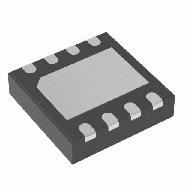
STMicroelectronics L99BM1T-TR
- Part No.:
- L99BM1T-TR
- Manufacturer:
- STMicroelectronics
- Category:
- Drivers, Receivers, Transceivers
- Package:
- 16-SOIC (0.154", 3.90mm Width)
- Datasheet:
-
 L99BM1T-TR.pdf
- Description:
- IC TRANSCEIVER HALF 1/1 16SO
- Quantity:
- Payment:

- Shipping:

Inventory:1,000
Please send an inquiry. Send us your inquiry, and we will respond immediately.
Product details
Overview
L99BM1T-TR from STMicroelectronics is a general-purpose SPI-to-isolated-SPI transceiver enabling bidirectional communication across galvanic isolation barriers. It operates as either SPI Master (configurable clock at 250 kHz/1 MHz/4 MHz/8 MHz) or Slave (up to 10 MHz), supports transformer or capacitive isolation, and delivers isolated data rates of 333 kbps or 2.66 Mbps on its 2-wire VIF interface. It is natively compatible with L99BM114 for battery management systems.
For engineers reviewing the L99BM1T-TR datasheet, L99BM1T-TR pinout, L99BM1T-TR application, or L99BM1T-TR equivalent, key selection criteria include dual-voltage logic compatibility (3.3 V/5 V), NSLAVE-configurable SPI role, ISOFREQ-selectable isolated bit rate, DIS-driven wake-up capability, and AEC-Q100-qualified operation from −40 °C to 105 °C ambient.
Technical Context
The L99BM1T-TR implements asynchronous dual-domain SPI bridging using internal 16 MHz main and 32 kHz standby oscillators. Its FSM dynamically enables/disables peripheral buffers (SDO, SCK, NCS, BNE) based on NSLAVE latch state and operational mode-reducing current draw during idle or sleep.
Isolation-side signaling uses differential analog I/O (ISOP/ISOM) with programmable amplitude (TXAMP) and common-mode voltage (1.2 V typical), while digital I/Os feature Schmitt-trigger inputs with RC filtering (fCUT_DIG_IN) for EMI robustness. The device manages timing asynchrony between domains via internal FIFO buffering and frame-level handshaking (BNE flag).
Key Specifications
| Parameter | Value and Actual Design Meaning |
|---|---|
| VDD Supply Range | 4.5 V to 5.5 V - guaranteed full functionality including SPI and isolated interface operation |
| VIO Logic Supply | 3.0 V to 5.5 V - supports direct interfacing with 3.3 V or 5 V MCUs without level shifters |
| SPI Slave Clock | Up to 10 MHz - enables high-throughput command/response cycles in slave-mode BMS nodes |
| Isolated Bit Rate | 333 kbps or 2.66 Mbps - selectable via ISOFREQ pin; matches L99BM114 timing for seamless BMS daisy-chains |
| Standby Current | 64 μA max at VDD - achieved by disabling unused buffers and oscillators when DIS = high |
| Operating Temp | −40 °C to 105 °C - qualified per AEC-Q100 Grade 2 for under-hood and industrial battery pack environments |
| ESD Protection | ±4 kV HBM on ISOP/ISOM - ensures robustness against transient coupling in noisy high-voltage battery systems |
Pinout & Package
Package: SO-16 narrow (SO16N), RoHS-compliant, tape-and-reel delivery.
| Pin/Terminal | Circuit Role | Design Meaning |
|---|---|---|
| VDD (16) | Power Input | 5 V supply for internal logic and isolated SPI circuitry; must be decoupled near pin |
| VIO (1) | Logic Buffer Supply | Defines voltage level for SDO, SCK, SDI, NCS I/Os; connects to host MCU rail (3.3 V or 5 V) |
| NSLAVE (12) | Configuration Input | Latched at power-up to select SPI Master (VDD) or Slave (GND); disables input buffer after configuration |
| DIS (6) | Enable/Wake-up I/O | Open-drain input/output: pulled high to enter sleep; driven low by device to interrupt MCU on isolated SPI activity |
| ISOFREQ (7) | Isolation Speed Select | Digital input selecting 333 kbps (low) or 2.66 Mbps (high); sampled on NCS assertion in Slave mode |
| ISOP / ISOM (15/14) | Isolated Differential Pair | Analog terminals for transformer/capacitive isolation; require matched PCB routing and controlled impedance |
| BNE/CPOL (8) | Mode-Dependent Signal | Slave: BNE flag (RX buffer not empty); Master: CPOL input (SPI clock polarity); internal pull-down active |
| TXEN/CPHA (11) | Mode-Dependent Control | Slave: TX enable (disable to suppress TX during burst reads); Master: CPHA input (clock phase selection) |
Key Features
| Feature | Design Value |
|---|---|
| Dual-Voltage Logic Interface | VIO pin accepts 3.3 V or 5 V directly-eliminates external level shifters in mixed-rail systems |
| Configurable SPI Role | NSLAVE pin latched at power-up determines Master/Slave behavior-enables reuse in master controllers and slave sensors |
| Asynchronous Domain Bridging | Internal FIFO and BNE flag manage timing mismatch between non-synchronized clock domains-no external synchronization required |
| Low-Power Sleep Mode | 64 μA standby current with DIS high-achieved by disabling main oscillator and unused I/O buffers |
| AEC-Q100 Qualified | Qualified to Grade 2 (−40 °C to 105 °C) with ±4 kV HBM on isolation pins-meets automotive BMS reliability requirements |
Applications
| Battery Management Systems (BMS) | Industrial Isolated Sensor Networks |
|---|---|
Use Scenario: Daisy-chained cell monitoring ICs (e.g., L9963E) communicate with central BMS controller across >1 kV isolation barriers. IC Role / Device Role / Timing Role: SPI-to-isolated-SPI bridge providing galvanically isolated command/response transport between controller and slave nodes. Use Value: Native compatibility with L99BM114 ensures deterministic timing and CRC-aligned frame handling for safety-critical cell voltage reporting. | Use Scenario: Remote temperature/pressure sensors in hazardous zones transmit data to PLCs via isolated SPI over long cables. IC Role / Device Role / Timing Role: Isolation barrier transceiver converting standard SPI to robust differential VIF signaling immune to ground loops and EMI. Use Value: 2.66 Mbps fast mode enables sub-millisecond sensor update rates even with 10+ daisy-chained nodes. |
| Uninterruptible Power Supplies (UPS) | High-Voltage Energy Storage Systems |
Use Scenario: Communication between DC-link monitoring units and system controller in modular UPS inverters with floating DC buses. IC Role / Device Role / Timing Role: Bidirectional isolated SPI interface maintaining data integrity across >2.5 kV reinforced isolation barriers. Use Value: 333 kbps slow mode provides noise margin in electrically noisy inverter switching environments while preserving timing accuracy. | Use Scenario: Inter-module communication in containerized grid-scale battery racks where modules operate at different potentials. IC Role / Device Role / Timing Role: Voltage-domain bridging transceiver supporting both transformer and capacitive isolation topologies per module design. Use Value: Dual logic supply (VIO) allows direct connection to 3.3 V microcontrollers inside each module without additional regulators. |
Equivalent & Alternatives
The following parts are listed as comparable options for similar SPI-isolation bridge applications.
| Alternative Part | Technical Difference | Application Difference | Selection Advice |
|---|---|---|---|
| ADUM3481ARQZ | Quad-channel digital isolator with integrated SPI controller; no native SPI framing or BNE flag | Requires external MCU firmware to handle SPI protocol framing and buffer management | Choose when needing multiple isolated signals beyond SPI, but accept added software overhead |
| SI8641ED-B-IS | 4-channel digital isolator with separate SCLK/MOSI/MISO/SS lines; no VIF compression or configurable bit rate | Transmits raw SPI signals without frame-level abstraction-less efficient bandwidth usage on isolation channel | Prefer for simple point-to-point SPI extension where protocol awareness is unnecessary |
Compared with ADUM3481ARQZ and SI8641ED-B-IS, L99BM1T-TR uniquely integrates SPI protocol awareness (frame length 8–64 bits), hardware-managed FIFOs, and BNE-driven interrupt signaling-reducing MCU firmware complexity and improving real-time responsiveness in daisy-chained BMS architectures.
Availability
L99BM1T-TR is available at Aetrix Electronics and suitable for high-voltage battery packs, backup energy storage systems and UPS, and industrial communication networks requiring stable component supply across extended product lifecycles.
Supply support for L99BM1T-TR includes scheduled delivery planning, volume procurement assistance, BOM continuity management, traceable sourcing, and lifecycle availability coordination for OEM customers, industrial embedded developers, connected-device designers, and electronics production programs.
Manufacturer
STMicroelectronics is a global semiconductor leader headquartered in Geneva, Switzerland, designing and manufacturing microcontrollers, power management ICs, and automotive-grade analog devices.
L99BM1T belongs to ST's Automotive Power Discrete & Analog portfolio, engineered specifically for functional-safety-compliant battery monitoring and high-voltage system communication in EVs and energy storage.
FAQ
What is the purpose of the NSLAVE pin, and how must it be configured?
The NSLAVE pin is latched at power-up to permanently configure the device as SPI Master (NSLAVE = VDD) or Slave (NSLAVE = GND). It must be hard-wired before initial power-on and cannot be changed dynamically. Internal pull-down ensures safe default behavior if left floating, and the input buffer is disabled after latching to reduce leakage and EMI susceptibility.
How does the DIS pin function in both input and output modes?
DIS serves dual roles: as an input, pulling it high places the device into 64 μA sleep mode; as an output, the device drives it low for TDIS_PULLDOWN upon detecting isolated SPI activity in standby-triggering MCU interrupt or PMIC wake-up. An internal current limiter protects against external short-to-VDD faults, and RC filtering ensures noise immunity.
Can L99BM1T-TR interface directly with 3.3 V and 5 V MCUs simultaneously?
Yes-VIO pin accepts either 3.3 V or 5 V to set logic levels for SDO, SCK, SDI, and NCS, while VDD remains fixed at 5 V. This allows direct connection to 3.3 V microcontrollers without level shifters, and coexistence with 5 V peripherals on the same SPI bus when VIO = 5 V.
What isolation methods does L99BM1T-TR support, and what design considerations apply?
L99BM1T-TR supports both transformer-based and capacitive isolation on its ISOP/ISOM differential pair. For transformer isolation, use center-tapped or push-pull drivers matching 1.2 V common-mode and ≤2.5 V differential swing. For capacitive isolation, ensure matched trace lengths, 100 Ω differential impedance, and guard traces to minimize crosstalk-ST recommends layout guidelines from AN5024.
L99BM1T-TR Specifications
- Product attributes
- Attribute value
- Manufacturer:
- STMicroelectronics
- Series:
- -
- Package/Case:
- 16-SOIC (0.154", 3.90mm Width)
- Packaging:
- Tape & Reel (TR)
- Product Status:
- Active
- Type:
- Transceiver, Isolated
- Protocol:
- -
- Number of Drivers/Receivers:
- 1/1
- Duplex:
- Half
- Receiver Hysteresis:
- 150 mV
- Data Rate:
- 2.66Mbps
- Voltage - Supply:
- 4.5V ~ 5.5V
- Operating Temperature:
- -40°C ~ 105°C (TA)
- Grade:
- -
- Qualification:
- -
- Mounting Type:
- Surface Mount
- Supplier Device Package:
- 16-SO
L99BM1T-TR FAQ
1.How can I place an order for L99BM1T-TR through Aetrix?
Please submit a Request for Quotation (RFQ) for L99BM1T-TR on Aetrix. Our sales agent will provide a competitive quotation and guide you through the order confirmation once you accept the terms.
2.Are the price and stock information for L99BM1T-TR reliable?
The price and inventory of L99BM1T-TR are updated periodically and may fluctuate due to market conditions. Stock and pricing data are typically refreshed every 24 hours. Quotation validity for L99BM1T-TR is usually 5 days.
3.What payment methods are accepted for L99BM1T-TR?
We accept Wire Transfer, PayPal, Credit Card, Western Union, MoneyGram, and Escrow for L99BM1T-TR transactions.
Note: Certain payment methods may incur a processing fee.
4.How is shipping managed for L99BM1T-TR?
L99BM1T-TR orders can be shipped via leading logistics carriers, including DHL, UPS, FedEx, TNT, or Registered Mail.
Once your L99BM1T-TR order is processed, you will receive an email with the shipment details and tracking number.
Note: Tracking information may take up to 24 hours to appear. Express delivery typically takes 3–5 business days.
5.How can I obtain technical support or documentation for L99BM1T-TR?
For technical support, including L99BM1T-TR datasheets, pinout diagrams, or application guidance, please contact our engineering support team. They can provide detailed documentation and assistance for your L99BM1T-TR requirements.
6.How does Aetrix verify that L99BM1T-TR is sourced from the original manufacturer or authorized distributors?
All L99BM1T-TR products on Aetrix are procured from qualified distributors and authorized channels. Our dedicated quality assurance team conducts strict verification, including traceability checks and, if necessary, third-party testing. This ensures that L99BM1T-TR meets industry standards.
7.What is the process for return or replacement of L99BM1T-TR?
All L99BM1T-TR units undergo pre-shipment inspection (PSI). If there is an issue with L99BM1T-TR, returns or replacements are accepted under the following conditions:
1.Quantity discrepancies, incorrect items, or visible external defects (such as breakage or corrosion), acknowledged by Aetrix.
2.The issue is reported within 90 days of delivery.
3.The L99BM1T-TR part is unused and in its original packaging.
Return procedure for L99BM1T-TR:
1.Submit a request within 90 days.
2.Obtain a Return Material Authorization (RMA) from Aetrix.
L99BM1T-TR Tags

-
ATA6561-GAQW-N
Microchip Technology
-
ATA6561-GBQW-N
Microchip Technology

-
AM26LS32ACDR
Texas Instruments

-
SP485CN-L/TR
MaxLinear, Inc.
-
SP485EN-L/TR
MaxLinear, Inc.
-
SP485EEN-L/TR
MaxLinear, Inc.
-
SP485ECN-L/TR
MaxLinear, Inc.
-
THVD1400DR
Texas Instruments
-
AM26C31IDR
Texas Instruments

-
TLIN1021ADRQ1
Texas Instruments
-
MAX232IDR
Texas Instruments
-
AM26C32IDR
Texas Instruments
Tech Hub

An engineering guide to LED driver operation, constant-current and constant-voltage outputs, linear and switching topologies, dimming, IC selection, calculations, replacement compatibility, and fault c…

Operational amplifier guide covering op amp basics, feedback, ideal vs real op amps, common configurations, buffer circuits, offset, bias current, gain-bandwidth, slew rate, rail-to-rail limits and sel…

Jumper cables guide covering safe connection order, red and black clamp placement, final ground connection, cable gauge, length, clamp quality, copper vs CCA cables, jump starter comparison and battery…

LDO regulator guide covering low dropout voltage, power dissipation, thermal design, PSRR, output noise, capacitor stability, adjustable LDO circuits, LDO vs buck converter and datasheet selection chec…

Conditional Access Module guide covering CAM meaning, CI/CI+ interface, smart card authorization, DVB security workflow, TV and set-top box compatibility, internal electronics, ESD protection, connecto…

Guide to electronic component obsolescence covering EOL risk, PCN/PDN notices, last-time buy planning, replacement options, form-fit-function validation, counterfeit risk and BOM lifecycle management.

18650 battery guide covering lithium-ion cell basics, 3.6V/3.7V voltage, 4.2V charging, mAh and Wh capacity, protected cells, chargers, BMS, series-parallel packs, holders, welding and sourcing checks.…

Hall effect sensor guide covering working principle, linear and digital sensors, Arduino circuits, current sensing, speed detection, automotive applications, A3144 examples, signal filtering and datash…

Product Change Notification guide for electronic components, covering PCN meaning, PCN vs PDN/EOL, common change types, risk levels, form-fit-function review, engineering validation, BOM control, LTB/L…

A practical guide to blend door actuators, covering HVAC function, symptoms, location, AC and heater issues, reset and calibration, replacement cost, electrical diagnosis, compatibility checks, and rep…


