
 My Inquiry
 My Account


STMicroelectronics L99LD02Q505
- Part No.:
- L99LD02Q505
- Manufacturer:
- STMicroelectronics
- Category:
- DC DC Switching Controllers
- Package:
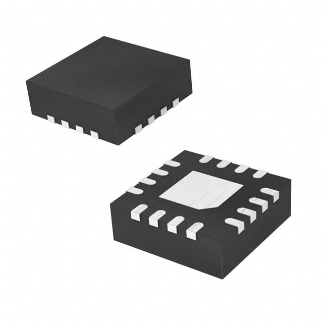
- 32-VFQFN Exposed Pad
- Datasheet:
-
 L99LD02Q505.pdf
- Description:
- DUAL-PHASE BOOST DC/DC CONTROLLE
- Quantity:
- Payment:

- Shipping:

Inventory:1,754
Please send an inquiry. Send us your inquiry, and we will respond immediately.
Product details
Overview
L99LD02Q505 from STMicroelectronics is an AEC-Q100 qualified automotive dual-phase boost DC/DC controller in QFN32L 5×5 package, driving N-channel MOSFETs with peak current mode control, programmable 100–470 kHz switching frequency, up to 80 V regulated output, and integrated 10 V gate driver LDO - designed for LED module power supplies in vehicle lighting systems.
For engineers reviewing the L99LD02Q505 datasheet, L99LD02Q505 pinout, L99LD02Q505 application, or L99LD02Q505 equivalent, key selection considerations include cold-cranking robustness, SPI-configurable input current limiting, multi-phase synchronization via SYNC_I/O, and Limp Home stand-alone operation without microcontroller dependency.
Technical Context
The L99LD02Q505 implements a fixed-frequency, peak current mode boost architecture with two independent phase channels, each featuring dedicated COMP error amplifier outputs, SP/SN current-sense inputs, and GO gate driver outputs. Its internal 10 V LDO powers standard-level MOSFET gates, while VS supply supports 3–28 V battery input range including cold crank (down to 3 V).
SPI v4.1 interface enables full runtime configuration of operating frequency, slope compensation, OVP threshold, thermal warning level, and limp-home behavior. The SYNC_I/O pin supports master/slave clock distribution with programmable phase shift for 2–4 phase interleaving, reducing output ripple and passive component stress.
Key Specifications
| Parameter | Value and Actual Design Meaning |
|---|---|
| Input Voltage Range | 3 V to 28 V - supports full automotive battery range including cold cranking (3 V) and load dump transients. |
| Boost Output Voltage | Up to 80 V - enables direct drive of high-voltage LED strings (e.g., 60 V nominal automotive headlamp arrays). |
| Switching Frequency | 100–470 kHz, programmable via SPI - balances EMI performance, efficiency, and magnetics size across vehicle platforms. |
| Gate Driver Supply | Integrated 10 V LDO - ensures reliable turn-on of standard-threshold N-channel MOSFETs without external bias rails. |
| Current Sensing | Dual SP/SN differential inputs per phase - enables accurate, noise-immune peak current mode control with external shunt resistors. |
| Protection Features | Programmable input overcurrent, thermal warning/shutdown, overvoltage protection, and VS undervoltage lockout - meets ASIL-B system-level safety requirements. |
| Communication Interface | ST SPI v4.1 (CSN/SCK/SDI/SDO) - provides register-level diagnostics, fault logging, and real-time parameter tuning without MCU firmware changes. |
Pinout & Package
Package: QFN32L 5×5 mm, 0.5 mm pitch, exposed thermal pad (PGND-connected) - optimized for automotive thermal cycling and board-level reliability under under-hood conditions.
| Pin/Terminal | Circuit Role | Design Meaning |
|---|---|---|
| VS (Pin 2) | Main IC supply input | Accepts 3–28 V battery rail; includes internal UVLO and cold-crank support; requires Schottky reverse polarity protection. |
| GO1 / GO2 (Pins 23, 21) | Phase 1/2 gate drivers | 10 V CMOS outputs driving external N-MOSFET gates; slew-rate controlled for EMI reduction. |
| SP1/SN1, SP2/SN2 (Pins 28/27, 18/19) | Differential current sense inputs | High-common-mode rejection inputs for external shunt-based peak current sensing per phase. |
| COMP1 / COMP2 (Pin 4, shared) | Error amplifier output | Single COMP pin serves both phases; external RC network sets loop stability and transient response. |
| SYNC_I/O (Pin 10) | Multi-phase clock interface | Configurable as master (generates phase-shifted clock) or slave (accepts external sync); enables 2–4 phase interleaving. |
| V10V (Pin 26) | Gate driver LDO output | Stable 10 V supply for MOSFET gates; requires local 1 µF low-ESR ceramic capacitor. |
| V3V3A / V3V3D (Pins 5, 6) | Digital logic supply outputs | 3.3 V regulated supplies for internal logic and SPI I/O; decoupled with 1 µF capacitors. |
| CSN / SCK / SDI / SDO (Pins 11–14) | SPI interface signals | CMOS-compatible, 3.3 V tolerant; supports daisy-chain configuration and fault detection (clock monitor, data stuck, CSN timeout). |
Key Features
| Feature | Design Value |
|---|---|
| Stand-alone Limp Home mode | Fully configurable via OTP bits - enables safe degraded operation (e.g., reduced LED brightness) during MCU failure or communication loss. |
| Programmable input current limit | Set via SPI register; uses external resistor ladder on SP/SN pins - prevents battery overload during startup or fault conditions. |
| Dither oscillator | Configurable frequency modulation depth and deviation % - reduces conducted and radiated EMI peaks without sacrificing regulation accuracy. |
| Thermal management | Two-stage thermal response: warning flag at 145 °C, shutdown at 165 °C - enables graceful system derating before catastrophic failure. |
| Device supply from boost output | Enables operation when battery drops below 5 V - maintains gate drive and control logic during cold crank, ensuring LED illumination continuity. |
Applications
| Automotive Front Headlamps | Commercial Vehicle Rear Lighting |
|---|---|
|
Use Scenario: High-brightness LED arrays requiring 48–60 V regulated supply in adaptive front-lighting systems (AFS). IC Role / Device Role / Timing Role: Dual-phase boost controller regulating output voltage while balancing current between two parallel boost stages via SYNC_I/O phase shift. Use Value: Reduces output capacitor size by 40% vs. single-phase design and maintains stable illumination during 6 V cold-crank events. |
Use Scenario: Modular LED brake/tail lamp assemblies in trucks and buses with variable string count (1–4 strings). IC Role / Device Role / Timing Role: Programmable boost controller supporting dynamic output voltage adjustment (40–80 V) via SPI to match changing LED forward voltage across temperature and aging. Use Value: Eliminates need for multiple BOM variants; one L99LD02Q505 design covers all rear lamp configurations. |
| Motorcycle Daytime Running Lights (DRL) | Off-Road Vehicle Work Lights |
|
Use Scenario: Compact, thermally constrained DRL modules powered directly from 12 V battery with wide ambient temperature range (−40 °C to +105 °C). IC Role / Device Role / Timing Role: Stand-alone Limp Home controller maintaining minimum LED output during MCU reset or CAN bus interruption. Use Value: Meets UN Regulation 148 functional safety requirement for continuous DRL operation without host processor dependency. |
Use Scenario: High-power auxiliary lighting (≥100 W) on agricultural and construction equipment subject to vibration and voltage transients. IC Role / Device Role / Timing Role: Two L99LD02Q505 devices stacked in 4-phase interleaved mode, synchronized via SYNC_I/O to reduce input/output ripple current. Use Value: Enables use of smaller, lower-cost 12 V input capacitors and extends electrolytic capacitor lifetime by 3× under 85 °C operation. |
Equivalent & Alternatives
The following parts are listed as comparable options for similar dual-phase boost controller applications.
| Alternative Part | Technical Difference | Application Difference | Selection Advice |
|---|---|---|---|
| LM5122MTX/NOPB | Single-phase controller; no integrated LDO or SPI interface; analog-only configuration via resistors. | Requires external 10 V bias supply and discrete current sense amplifiers; lacks limp-home or diagnostic capability. | Lower BOM cost for non-safety-critical, fixed-function designs without software configurability needs. |
| MAX20077ATP/VY+ | Single-phase, 60 V max output; integrates 5 V LDO only; no multi-phase sync or cold-crank support below 4.5 V. | Not qualified for AEC-Q100 Grade 1; limited to cabin lighting or infotainment displays, not exterior lighting. | Valid for interior LED backlighting where extended temperature and cold-crank are not required. |
Compared with LM5122MTX/NOPB and MAX20077ATP/VY+, the L99LD02Q505 uniquely delivers AEC-Q100 Grade 1 compliance, dual-phase interleaving with SYNC_I/O, cold-crank down to 3 V, and SPI-configurable limp-home - making it the only solution qualified for ASIL-B exterior lighting control.
Availability
L99LD02Q505 is available at Aetrix Electronics and suitable for automotive LED lighting, off-road vehicle work lights, and motorcycle DRL systems requiring stable component supply, long-term lifecycle assurance, and AEC-Q100-compliant sourcing.
Supply support for L99LD02Q505 includes scheduled delivery planning, volume procurement assistance, BOM continuity management, traceable sourcing, and lifecycle availability coordination for OEM customers, industrial embedded developers, connected-device designers, and electronics production programs.
Manufacturer
STMicroelectronics is a global semiconductor leader headquartered in Geneva, Switzerland, specializing in automotive-grade power management, microcontrollers, and analog ICs with vertical manufacturing and AEC-Q100 validation infrastructure.
The L99LD02Q505 belongs to ST's automotive LED driver controller product line, engineered specifically for high-reliability, software-defined exterior lighting systems requiring functional safety, multi-phase scalability, and cold-crank resilience.
FAQ
What is the minimum input voltage supported during cold cranking?
The L99LD02Q505 operates down to 3 V on the VS pin, enabling uninterrupted LED illumination during automotive cold-cranking events. This is achieved through internal UVLO hysteresis and boosted gate drive derived from the BST_OUT rail when battery voltage falls below 5 V.
How does the SYNC_I/O pin enable multi-phase operation?
SYNC_I/O functions as a bidirectional clock interface: in master mode, it outputs a programmable phase-shifted clock signal to synchronize additional L99LD02 devices; in slave mode, it accepts an external clock. This allows precise 90° or 120° phase shifts across 2–4 phases to minimize input/output ripple.
Can the L99LD02Q505 operate without an MCU?
Yes - its Limp Home mode is fully configurable via OTP bits and supports stand-alone operation with pre-programmed parameters (frequency, OVP, current limit). It retains critical functionality such as overtemperature warning, input overcurrent protection, and regulated output even during SPI communication loss or MCU reset.
What external components are mandatory for basic operation?
Mandatory components include: two external N-channel MOSFETs (one per phase), two current-sense shunts (SP/SN connections), output inductor and capacitor, bootstrap diode/capacitor for gate drive, 1 µF ceramic capacitor on V10V, and 1 µF capacitors on V3V3A/V3V3D. No external error amplifier compensation is required for default stability.
L99LD02Q505 Specifications
- Product attributes
- Attribute value
- Manufacturer:
- STMicroelectronics
- Series:
- -
- Package/Case:
- 32-VFQFN Exposed Pad
- Packaging:
- Tray
- Product Status:
- Obsolete
- Output Type:
- Transistor Driver
- Function:
- Step-Up
- Output Configuration:
- Positive
- Topology:
- Boost
- Number of Outputs:
- 1
- Output Phases:
- 2
- Voltage - Supply (Vcc/Vdd):
- 3V ~ 28V
- Frequency - Switching:
- 100kHz ~ 470kHz
- Duty Cycle (Max):
- 95%
- Synchronous Rectifier:
- No
- Clock Sync:
- Yes
- Serial Interfaces:
- SPI
- Control Features:
- Current Limit, Enable, Frequency Control, Phase Control, Power Good, Ramp, Soft Start, Watchdog
- Operating Temperature:
- -40°C ~ 150°C (TJ)
- Grade:
- Automotive
- Qualification:
- AEC-Q100
- Mounting Type:
- Surface Mount, Wettable Flank
- Supplier Device Package:
- 32-QFN (5x5)
L99LD02Q505 FAQ
1.How can I place an order for L99LD02Q505 through Aetrix?
Please submit a Request for Quotation (RFQ) for L99LD02Q505 on Aetrix. Our sales agent will provide a competitive quotation and guide you through the order confirmation once you accept the terms.
2.Are the price and stock information for L99LD02Q505 reliable?
The price and inventory of L99LD02Q505 are updated periodically and may fluctuate due to market conditions. Stock and pricing data are typically refreshed every 24 hours. Quotation validity for L99LD02Q505 is usually 5 days.
3.What payment methods are accepted for L99LD02Q505?
We accept Wire Transfer, PayPal, Credit Card, Western Union, MoneyGram, and Escrow for L99LD02Q505 transactions.
Note: Certain payment methods may incur a processing fee.
4.How is shipping managed for L99LD02Q505?
L99LD02Q505 orders can be shipped via leading logistics carriers, including DHL, UPS, FedEx, TNT, or Registered Mail.
Once your L99LD02Q505 order is processed, you will receive an email with the shipment details and tracking number.
Note: Tracking information may take up to 24 hours to appear. Express delivery typically takes 3–5 business days.
5.How can I obtain technical support or documentation for L99LD02Q505?
For technical support, including L99LD02Q505 datasheets, pinout diagrams, or application guidance, please contact our engineering support team. They can provide detailed documentation and assistance for your L99LD02Q505 requirements.
6.How does Aetrix verify that L99LD02Q505 is sourced from the original manufacturer or authorized distributors?
All L99LD02Q505 products on Aetrix are procured from qualified distributors and authorized channels. Our dedicated quality assurance team conducts strict verification, including traceability checks and, if necessary, third-party testing. This ensures that L99LD02Q505 meets industry standards.
7.What is the process for return or replacement of L99LD02Q505?
All L99LD02Q505 units undergo pre-shipment inspection (PSI). If there is an issue with L99LD02Q505, returns or replacements are accepted under the following conditions:
1.Quantity discrepancies, incorrect items, or visible external defects (such as breakage or corrosion), acknowledged by Aetrix.
2.The issue is reported within 90 days of delivery.
3.The L99LD02Q505 part is unused and in its original packaging.
Return procedure for L99LD02Q505:
1.Submit a request within 90 days.
2.Obtain a Return Material Authorization (RMA) from Aetrix.
L99LD02Q505 Tags

-
UCC28C45DR
Texas Instruments
-
UCC28C40DR
Texas Instruments
-
UCC28C43DR
Texas Instruments

-
ZXSC410E6TA
Diodes Incorporated

-
LM3524DMX/NOPB
Texas Instruments

-
LM3489MMX/NOPB
Texas Instruments
-
MIC2102YML-TR
Microchip Technology

-
LM5148RGYR
Texas Instruments
-
TL598CDR
Texas Instruments

-
LM5155DSSR
Texas Instruments

-
LM25085MYX/NOPB
Texas Instruments
-
UCC2813DTR-0
Texas Instruments
Tech Hub

Operational amplifier guide covering op amp basics, feedback, ideal vs real op amps, common configurations, buffer circuits, offset, bias current, gain-bandwidth, slew rate, rail-to-rail limits and sel…

Jumper cables guide covering safe connection order, red and black clamp placement, final ground connection, cable gauge, length, clamp quality, copper vs CCA cables, jump starter comparison and battery…

LDO regulator guide covering low dropout voltage, power dissipation, thermal design, PSRR, output noise, capacitor stability, adjustable LDO circuits, LDO vs buck converter and datasheet selection chec…

Conditional Access Module guide covering CAM meaning, CI/CI+ interface, smart card authorization, DVB security workflow, TV and set-top box compatibility, internal electronics, ESD protection, connecto…

Guide to electronic component obsolescence covering EOL risk, PCN/PDN notices, last-time buy planning, replacement options, form-fit-function validation, counterfeit risk and BOM lifecycle management.

18650 battery guide covering lithium-ion cell basics, 3.6V/3.7V voltage, 4.2V charging, mAh and Wh capacity, protected cells, chargers, BMS, series-parallel packs, holders, welding and sourcing checks.…

Hall effect sensor guide covering working principle, linear and digital sensors, Arduino circuits, current sensing, speed detection, automotive applications, A3144 examples, signal filtering and datash…

Product Change Notification guide for electronic components, covering PCN meaning, PCN vs PDN/EOL, common change types, risk levels, form-fit-function review, engineering validation, BOM control, LTB/L…

A practical guide to blend door actuators, covering HVAC function, symptoms, location, AC and heater issues, reset and calibration, replacement cost, electrical diagnosis, compatibility checks, and rep…

Engineering guide to Raspberry Pi alternatives, covering chip-level differences, Orange Pi, ROCK, Jetson, Banana Pi, NanoPi, Compute Module, Pico, GPIO, camera, HAT compatibility, and replacement risks…


