Send an Inquiry

To receive a quote for your project, please fill in the following information, and we’ll get back to you promptly.

Name*
Company*
Email Address*
Phone/WhatsApp
Part Number*
Quantity*
Message
Submit Inventory List

Please fill in the following information, and we’ll get back to you promptly.

Name*
Company*
Email Address*
Phone/WhatsApp
Upload My List
Message

STMicroelectronics LD57100J800R

Part No.:
LD57100J800R
Manufacturer:
STMicroelectronics
Category:
Voltage Regulators - Linear, Low Drop Out (LDO) Regulators
Package:
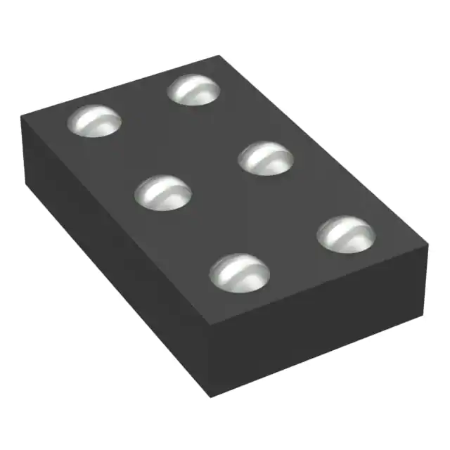
6-XFBGA, FCBGA
Datasheet:
AetrixLD57100J800R.pdf
Description:
IC REG LINEAR 0.8V 1A 6FLIPCHIP
Quantity:
Payment:
Payment
Shipping:
Shipping

Inventory:498

Please send an inquiry. Send us your inquiry, and we will respond immediately.

Part Number
Quantity*
Price
Name*
Company
Email*
Comments

Product details

Overview

LD57100J800R from STMicroelectronics is a fixed-output 0.8 V, 1 A ultra-low-dropout linear regulator (LDO) with NMOS pass transistor and dedicated VBIAS pin for sub-1 V operation. It delivers ±1% output accuracy over −40 °C to +85 °C, 40 mV dropout at 1 A load, and 35 μA ground current at no load-enabling high-efficiency post-regulation in space-constrained battery-powered systems such as smartphone core logic rails.

For engineers reviewing the LD57100J800R datasheet, LD57100J800R pinout, LD57100J800R application, or LD57100J800R equivalent, key selection criteria include bias-supply flexibility (3.0–5.5 V), active output discharge, thermal shutdown (160 °C), and Flip Chip6 package compatibility with low-noise ceramic output capacitors (≥1 µF, X5R/X7R).

Technical Context

The LD57100J800R employs an NMOS pass element driven by a separate VBIAS supply, decoupling control circuitry from VIN to sustain ultra-low dropout even when VIN approaches VOUT (e.g., 0.8 V). Its internal reference (0.5 V) and feedback network are optimized for fixed 0.8 V output with ±0.5% tolerance at 25 °C and ±1% across full temperature range.

It integrates logic-controlled enable (EN), thermal shutdown with 20 °C hysteresis, current limiting (1.5–2.6 A), and an internal discharge MOSFET (RON = 150 Ω) activated during shutdown. Supply rejection exceeds 75 dB (VIN) and 85 dB (VBIAS) at 1 kHz, while output noise is 27 µVRMS (10 Hz–100 kHz) for fixed versions.

Key Specifications

Parameter Value and Actual Design Meaning
Output voltage Fixed 0.8 V - matches core voltage requirements of modern ARM Cortex-A/M processors and LPDDR I/O rails.
Max output current 1 A guaranteed - supports high-transient digital loads without external current boosting.
Dropout voltage 40 mV typ. at 1 A - enables regulation from 0.84 V input, critical for single-cell Li-ion or Li-poly backup power paths.
Output accuracy ±1% over −40 °C to +85 °C - ensures stable core voltage under thermal stress in handheld enclosures.
Ground current 35 μA typ. at no load - minimizes quiescent drain in always-on subsystems (e.g., RTC, sensor hubs).
VBIAS range 3.0 V to 5.5 V, or ≥ VOUT + 1.6 V - allows flexible bias sourcing from system PMIC rails or shared 3.3 V/5 V supplies.
Enable threshold Logic-high ≥ 0.9 V - compatible with 1.2 V, 1.8 V, and 3.3 V GPIOs without level-shifting.
Thermal shutdown 160 °C typical - protects against sustained overload in thermally isolated PCB layouts.

Pinout & Package

LD57100J800R is housed in a Flip Chip6 package (0.8 mm × 1.2 mm, 0.4 mm pitch), optimized for minimal PCB footprint and thermal performance (RthJA = 60 °C/W on standard 4-layer JEDEC board). The die-down construction enables direct thermal coupling to inner copper planes.

Pin/Terminal Circuit Role Design Meaning
VOUT Regulated output Delivers stable 0.8 V to load; requires ≥1 µF X5R/X7R ceramic capacitor placed adjacent to pin.
SNS Output voltage sense Separate Kelvin connection for fixed version - routed directly to load to compensate PCB IR drop.
GND Power and signal reference Common return for VIN, VBIAS, EN, and SNS; must connect to low-impedance analog ground plane.
EN Enable control input Active-high logic interface; pulls device into <0.1 µA shutdown state when driven low.
VIN Main input supply Accepts 0.6–5.5 V; minimum headroom = VDROP + VOUT (e.g., 0.84 V for 0.8 V output).
VBIAS Bias supply input Powers internal gate driver and control circuitry; must be ≥3.0 V and ≥VOUT + 1.6 V for NMOS gate overdrive.

Key Features

Feature Design Value
Ultra-low dropout 40 mV at 1 A load - sustains regulation down to 0.84 V input, enabling use with depleted batteries or low-headroom sources.
Active output discharge Integrated 150 Ω MOSFET - discharges VOUT to GND within microseconds upon EN deactivation, preventing floating rail issues in multi-rail sequencing.
High PSRR 85 dB @ 1 kHz on VBIAS, 75 dB @ 1 kHz on VIN - suppresses ripple from noisy PMIC switchers feeding the bias or main input rails.
Low-noise output 27 µVRMS (10 Hz–100 kHz) - meets stringent noise budgets for RF transceivers and high-speed SerDes receivers powered from this LDO.
Thermal & current protection 160 °C shutdown with 20 °C hysteresis + 1.5–2.6 A current limit - prevents damage during short-circuit or thermal runaway events.
Small-footprint packaging Flip Chip6 (0.8 × 1.2 mm) - reduces layout area by >50% vs. comparable SOT-563 or DFN packages, easing routing in dense mobile PCBs.

Applications

Smartphone Core Rail Camera Sensor Power

Use Scenario: Regulating 0.8 V supply for application processor big.LITTLE clusters during DVFS transitions.

IC Role / Device Role / Timing Role: Primary post-regulator delivering clean, fast-response voltage to CPU/GPU cores.

Use Value: 40 mV dropout and 160 µs turn-on time minimize voltage droop during sudden 0–1 A load steps, maintaining timing margin.

Use Scenario: Powering high-resolution CMOS image sensor analog front-end (AFE) and PLL circuits.

IC Role / Device Role / Timing Role: Low-noise, low-ripple LDO supplying critical analog and clock domains.

Use Value: 27 µVRMS output noise and 85 dB VBIAS PSRR prevent spurious artifacts and jitter in image capture and video streaming.

Wearable SoC I/O LPDDR Memory Interface

Use Scenario: Providing 0.8 V to wearable ASIC I/O banks interfacing with BLE/Wi-Fi radios and touch controllers.

IC Role / Device Role / Timing Role: Compact, low-quiescent LDO enabling always-on sensing with sub-µA standby current.

Use Value: 35 µA no-load ground current and <0.1 µA shutdown current extend battery life in multi-day wearables.

Use Scenario: Supplying 0.8 V to LPDDR4/5 memory VDDQ rails in thin-profile tablets and ultrabooks.

IC Role / Device Role / Timing Role: High-current, low-ESR-stable LDO supporting high-speed DDR data eye integrity.

Use Value: Stable operation with 1 µF X7R ceramic output capacitor ensures robust transient response during burst read/write cycles.

Equivalent & Alternatives

The following parts are listed as comparable options for similar ultra-low-dropout LDO applications.

Alternative Part Technical Difference Application Difference Selection Advice
Torex XC6210B082MR-G Fixed 0.8 V, 1 A, 60 mV dropout (typ.), no VBIAS pin, SOT-25 package (2.9 × 2.8 mm) Larger footprint, higher dropout limits use below 0.86 V input; lacks active discharge and bias-supply flexibility. Select when board space permits larger package and bias rail sharing is not required.
Richtek RT9080L-08GJ5 Fixed 0.8 V, 1 A, 55 mV dropout (typ.), integrated soft-start, WDFN-6L (1.2 × 1.2 mm) No VBIAS pin; lower PSRR (70 dB @ 1 kHz); no output discharge; slightly larger footprint than Flip Chip6. Prefer when soft-start is mandatory and thermal performance is secondary to cost.

Compared with XC6210B082MR-G and RT9080L-08GJ5, LD57100J800R uniquely combines sub-50 mV dropout, VBIAS-enabled ultra-low-input operation, active discharge, and the smallest available footprint-making it optimal for next-gen mobile SoC power delivery where input headroom, board area, and rail sequencing are tightly constrained.

Availability

LD57100J800R is available at Aetrix Electronics and suitable for smartphone core rails, camera sensor power, wearable SoC I/O, and LPDDR memory interfaces requiring stable component supply, long-term lifecycle support, and consistent parametric performance across production batches.

Supply support for LD57100J800R includes scheduled delivery planning, volume procurement assistance, BOM continuity management, traceable sourcing, and lifecycle availability coordination for OEM customers, industrial embedded developers, connected-device designers, and electronics production programs.

Manufacturer

STMicroelectronics is a global semiconductor leader headquartered in Geneva, Switzerland, designing and manufacturing microcontrollers, power management ICs, sensors, and analog devices for automotive, industrial, and consumer markets.

LD57100J800R belongs to ST's high-accuracy, ultra-low-dropout LDO family engineered specifically for advanced mobile and portable electronics demanding minimal voltage headroom, nanoscale footprints, and robust protection features.

FAQ

Can LD57100J800R operate with VIN equal to VOUT?

No. Minimum VIN is VOUT + VDROP, which is 0.84 V (0.8 V + 40 mV typ.) at 1 A load. Below this, regulation fails and output collapses. The VBIAS pin must also be ≥3.0 V or ≥VOUT + 1.6 V (≥2.4 V), so practical minimum VIN is governed by whichever requirement is larger - typically VBIAS constraint dominates at very low VOUT.

What is the purpose of the separate SNS pin?

The SNS (sense) pin provides Kelvin feedback for the fixed-output version, allowing the regulator to monitor voltage directly at the load rather than at the VOUT pin. This compensates for IR drop across PCB traces, ensuring ±1% accuracy at the point-of-load - essential for precision core rails where even 10 mV error impacts timing margins.

Is an external capacitor required on the VBIAS pin?

Yes. A minimum 100 nF ceramic capacitor (X5R/X7R) must be placed between VBIAS and GND, located as close as possible to the pin. This stabilizes the bias supply for the internal gate driver and prevents oscillation or erratic enable behavior under dynamic load conditions.

Does LD57100J800R support reverse current blocking?

No. The NMOS pass transistor architecture does not provide inherent reverse current blocking. If reverse current flow from VOUT to VIN is possible in the system (e.g., during hot-swap or partial power-down), an external Schottky diode or ideal diode controller must be added in series with VIN.

LD57100J800R Specifications

Product attributes
Attribute value
Manufacturer:
STMicroelectronics
Series:
-
Package/Case:
6-XFBGA, FCBGA
Packaging:
Tape & Reel (TR)
Product Status:
Active
Output Configuration:
Positive
Output Type:
Fixed
Number of Regulators:
1
Voltage - Input (Max):
5.5V
Voltage - Output (Min/Fixed):
0.8V
Voltage - Output (Max):
-
Voltage Dropout (Max):
0.08V @ 1A
Current - Output:
1A
Current - Quiescent (Iq):
50 µA
Current - Supply (Max):
-
PSRR:
75dB (1kHz)
Control Features:
Enable
Protection Features:
Over Current, Over Temperature
Operating Temperature:
-40°C ~ 85°C (TJ)
Grade:
-
Qualification:
-
Mounting Type:
Surface Mount
Supplier Device Package:
6-FlipChip (0.78x1.18)

LD57100J800R FAQ

1.How can I place an order for LD57100J800R through Aetrix?

Please submit a Request for Quotation (RFQ) for LD57100J800R on Aetrix. Our sales agent will provide a competitive quotation and guide you through the order confirmation once you accept the terms.

2.Are the price and stock information for LD57100J800R reliable?

The price and inventory of LD57100J800R are updated periodically and may fluctuate due to market conditions. Stock and pricing data are typically refreshed every 24 hours. Quotation validity for LD57100J800R is usually 5 days.

3.What payment methods are accepted for LD57100J800R?

We accept Wire Transfer, PayPal, Credit Card, Western Union, MoneyGram, and Escrow for LD57100J800R transactions.

Note: Certain payment methods may incur a processing fee.

4.How is shipping managed for LD57100J800R?

LD57100J800R orders can be shipped via leading logistics carriers, including DHL, UPS, FedEx, TNT, or Registered Mail.

Once your LD57100J800R order is processed, you will receive an email with the shipment details and tracking number.

Note: Tracking information may take up to 24 hours to appear. Express delivery typically takes 3–5 business days.

5.How can I obtain technical support or documentation for LD57100J800R?

For technical support, including LD57100J800R datasheets, pinout diagrams, or application guidance, please contact our engineering support team. They can provide detailed documentation and assistance for your LD57100J800R requirements.

6.How does Aetrix verify that LD57100J800R is sourced from the original manufacturer or authorized distributors?

All LD57100J800R products on Aetrix are procured from qualified distributors and authorized channels. Our dedicated quality assurance team conducts strict verification, including traceability checks and, if necessary, third-party testing. This ensures that LD57100J800R meets industry standards.

7.What is the process for return or replacement of LD57100J800R?

All LD57100J800R units undergo pre-shipment inspection (PSI). If there is an issue with LD57100J800R, returns or replacements are accepted under the following conditions:

1.Quantity discrepancies, incorrect items, or visible external defects (such as breakage or corrosion), acknowledged by Aetrix.

2.The issue is reported within 90 days of delivery.

3.The LD57100J800R part is unused and in its original packaging.

Return procedure for LD57100J800R:

1.Submit a request within 90 days.

2.Obtain a Return Material Authorization (RMA) from Aetrix.

LD57100J800R Tags

  • LD57100J800R
  • LD57100J800R PDF
  • LD57100J800R Datasheet
  • LD57100J800R Specifications
  • LD57100J800R Images
  • STMicroelectronics
  • STMicroelectronics LD57100J800R
  • Buy LD57100J800R
  • LD57100J800R Price
  • LD57100J800R Distributor
  • LD57100J800R Supplier
  • LD57100J800R Wholesale
Related Products
MIC5504-1.8YM5-TR
MIC5504-1.8YM5-TR

Microchip Technology

MIC5504-3.3YM5-TR
MIC5504-3.3YM5-TR

Microchip Technology

MIC5365-3.0YC5-TR
MIC5365-3.0YC5-TR

Microchip Technology

MIC5365-1.8YC5-TR
MIC5365-1.8YC5-TR

Microchip Technology

MIC5365-2.5YC5-TR
MIC5365-2.5YC5-TR

Microchip Technology

MIC5365-3.3YC5-TR
MIC5365-3.3YC5-TR

Microchip Technology

MIC5365-3.3YD5-TR
MIC5365-3.3YD5-TR

Microchip Technology

MIC5317-3.3YM5-TR
MIC5317-3.3YM5-TR

Microchip Technology

TLV1117LV33DCYR
TLV1117LV33DCYR

Texas Instruments

MIC5317-3.3YMT-TZ
MIC5317-3.3YMT-TZ

Microchip Technology

MIC5528-3.3YMT-TR
MIC5528-3.3YMT-TR

Microchip Technology

TLV75801PDRVR
TLV75801PDRVR

Texas Instruments

Tech Hub

Search

Search

PRODUCT

PRODUCT

PHONE

PHONE

USER

USER