
 My Inquiry
 My Account


Microchip Technology LE75183BFSCT
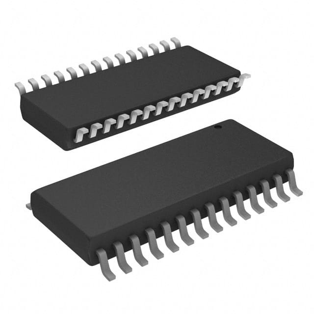
- Part No.:
- LE75183BFSCT
- Manufacturer:
- Microchip Technology
- Category:
- Telecom
- Package:
- 28-SOIC (0.295", 7.50mm Width)
- Datasheet:
-
 LE75183BFSCT.pdf
- Description:
- IC TELECOM INTERFACE 28SOIC
- Quantity:
- Payment:

- Shipping:

Inventory:1,258
Please send an inquiry. Send us your inquiry, and we will respond immediately.
Product details
Overview
LE75183BFSCT from Zarlink Semiconductor is a monolithic Line Card Access Switch (LCAS) providing solid-state equivalent functionality of three 2-form-C electromechanical relays. It delivers power ringing access, line test-out (loop access), and SLIC test-in switching for tip/ring in analog telephony line cards. Key confirmed parameters include 5 V only operation, <1.1 mA typical supply current in all-OFF state, >480 V breakdown rating on ringing access switch (SW8), and integrated thermal shutdown with battery-monitoring all-OFF fail-safe behavior.
For engineers reviewing the LE75183BFSCT datasheet, LE75183BFSCT pinout, LE75183BFSCT application, or LE75183BFSCT equivalent, this page provides verified technical context, exact pin functions per 32-pin QFN package, real-world telephony switching states (e.g., simultaneous test-in/test-out), protection architecture differences between A/C and B variants, and two validated alternative parts for central office and DLC line card designs.
Technical Context
The LE75183BFSCT implements seven discrete switching states via logic-level inputs (INRING, INTESTin, INTESTout, LATCH), supporting idle/talk, power ringing, loop access, SLIC test, simultaneous loop+SLIC access, ringing generator test, and all-OFF. Its internal architecture includes break-before-make or make-before-break control logic, diode bridge + current limiting + thermal shutdown (no SCR clamping), and dedicated TSD pin for thermal flagging or disable control.
It operates exclusively from 5 V (VDD = 4.5–5.5 V), draws ≤2.1 mA during power ringing, and uses VBAT (–72 to –19 V) solely as a reference for protection circuitry - loss of battery forces immediate all-OFF state. All switches feature <1 µA off-state leakage at ±330 V and dV/dt immunity up to 200 V/µs.
Key Specifications
| Parameter | Value and Actual Design Meaning |
|---|---|
| Supply Voltage | 5 V only (4.5–5.5 V); eliminates need for multi-rail supplies and enables ultra-low-power remote line card deployment. |
| All-OFF Supply Current | 0.76–1.1 mA typical; minimizes standby power in battery-backed central office applications. |
| Ringing Access Switch Breakdown | >480 V; withstands transient faults without external zero-cross circuitry when paired with foldback protector. |
| ON-Resistance Match (SW3/SW4) | ≤1.0 Ω mismatch; ensures balanced signal integrity across tip/ring paths in loop access mode. |
| Thermal Shutdown Flag | TSD pin outputs LOW during thermal shutdown; enables system-level fault reporting without external sensors. |
| Battery Monitor Behavior | Enters all-OFF state if VBAT rises above –10 V; prevents unsafe operation during battery degradation or disconnect. |
| Logic Input Compatibility | TTL-compatible with internal 75 kΩ pull-up/down; eliminates external biasing components for INRING (pull-up) and INTESTin (pull-down). |
Pinout & Package
LE75183BFSCT is packaged in a 32-pin QFN with exposed pad (EPAD), RoHS-compliant, lead-free matte-tin plating. The EPAD has no internal electrical connection and must be soldered to an equal-sized copper pad for mechanical stability only - no VBAT or ground connection recommended.
| Pin/Terminal | Circuit Role | Design Meaning |
|---|---|---|
| VDD | 5 V power supply input | Primary power rail; must be decoupled locally due to switching transients from 10+ solid-state switches. |
| VBAT | Battery voltage reference | Connects to –48 V battery; used only by internal protection circuit - not a power source. |
| DGND / FGND | Digital and fault ground | Separate ground returns prevent noise coupling between logic and high-voltage fault paths. |
| INRING / INTESTin / INTESTout / LATCH | Logic control inputs | Direct TTL-level interface; LATCH is active-high transparent latch enabling synchronous state updates. |
| TLINE / RLINE / TRINGING / RRINGING / TBAT / RBAT | TIP/RING line-side and SLIC-side terminals | High-voltage bidirectional I/O; rated for ±330 V isolation and 480 V breakdown on ringing path. |
| TTESTin / RTESTin / TTESTout / RTESTout | Test access points | Enable SLIC-side (test-in) and line-side (test-out) diagnostics without physical relay manipulation. |
| TSD | Thermal shutdown flag/control | Configurable as input (disable shutdown) or open-drain output (LOW = thermal trip); requires pull-up for output use. |
Key Features
| Feature | Design Value |
|---|---|
| Make-before-break / break-before-make switching | Prevents momentary open-circuit during ring cadence transitions, eliminating audible click/noise in voice path. |
| Integrated current limiting & thermal shutdown | Protects downstream SLIC and ringing generator during lightning surges or power cross without external circuitry. |
| Battery-loss all-OFF fail-safe | Guarantees line disconnection upon battery failure - critical for Telcordia GR-357 compliance in central office systems. |
| No external drive circuitry required | Latch and input pins have internal 75 kΩ pull resistors, reducing BOM count and PCB footprint in space-constrained line cards. |
| Single secondary protector requirement | One foldback/crowbar protector suffices for full tip/ring protection - simplifies layout and meets ITU-T K.21 requirements. |
Applications
| Central Office Line Card | Digital Loop Carrier (DLC) |
|---|---|
Use Scenario: Providing ringing access, loop testing, and SLIC diagnostics in Class 5 CO line cards serving POTS subscribers. IC Role / Device Role / Timing Role: Solid-state replacement for three EMRs, managing tip/ring connectivity across seven defined telephony states. Use Value: Eliminates mechanical wear, reduces impulse noise, and enables simultaneous test-in/test-out required for Telcordia TR-57 compliance. | Use Scenario: Remote terminal line cards in fiber-fed DLC systems where low power and high reliability are mandatory. IC Role / Device Role / Timing Role: Enables battery-backed operation with all-OFF fail-safe and <1.1 mA idle current for extended backup runtime. Use Value: Meets TA-909 remote power constraints while delivering same switching fidelity as central office deployments. |
| PBX Analog Interface | HFC/FITL Distribution Node |
Use Scenario: Analog station interface modules in enterprise PBX systems requiring clean, bounce-free switching for maintenance and diagnostics. IC Role / Device Role / Timing Role: Controls test access to SLIC and line side independently, supporting hot-swap diagnostics without service interruption. Use Value: Clean switching and low ON-resistance match (<1 Ω) preserve voice signal integrity during live-line testing. | Use Scenario: Hybrid fiber-coax nodes converting digital signals to analog POTS for last-mile delivery in FITL architectures. IC Role / Device Role / Timing Role: Manages ringing generator interface and line test paths under varying battery conditions in unattended outdoor cabinets. Use Value: Integrated battery monitor and thermal shutdown ensure autonomous fault containment without host MCU intervention. |
Equivalent & Alternatives
The following parts are listed as comparable options for similar line card access switch applications.
| Alternative Part | Technical Difference | Application Difference | Selection Advice |
|---|---|---|---|
| LE75183AFQC | Same 32-pin QFN package, but A version includes SCR clamping in protection circuit (B version does not). | Required where positive/negative lightning surge protection must be steered fully to ground (e.g., LSSGR Zone 1 deployments). | Select LE75183AFQC if SCR-based fault steering is mandated; otherwise LE75183BFSCT's diode-bridge-only scheme suffices for most DLC/PBX use cases. |
| LE75183BFSC | 28-pin SOIC package (larger footprint), identical B-version functionality and protection architecture. | Suitable for legacy board refreshes where 32-pin QFN rework is impractical but B-variant features are needed. | Choose LE75183BFSC only for drop-in replacement in existing 28-pin SOIC layouts; new designs should prefer LE75183BFSCT for size and thermal performance. |
Compared with LE75183AFQC, LE75183BFSCT omits SCR clamping - reducing complexity and cost where full bidirectional fault steering isn't required. Against LE75183BFSC, it delivers identical functionality in a smaller, thermally superior QFN package ideal for high-density line card designs.
Availability
LE75183BFSCT is available at Aetrix Electronics and suitable for central office, digital loop carrier, and PBX analog line card applications requiring stable component supply, long lifecycle support, and RoHS-compliant packaging.
Supply support for LE75183BFSCT includes scheduled delivery planning, volume procurement assistance, BOM continuity management, traceable sourcing, and lifecycle availability coordination for OEM customers, industrial embedded developers, connected-device designers, and electronics production programs.
Manufacturer
Zarlink Semiconductor was a fabless IC designer specializing in communications infrastructure semiconductors, later acquired by Microsemi (now Microchip). Known for high-reliability telecom solutions.
The LE75183BFSCT belongs to the VoiceEdge™ VE750 series, engineered specifically for solid-state replacement of electromechanical relays in analog telephony line cards - emphasizing low power, fail-safe behavior, and integrated protection.
FAQ
What is the primary function of the LE75183BFSCT in a telephony line card?
The LE75183BFSCT serves as a monolithic Line Card Access Switch that replaces three 2-form-C electromechanical relays. It manages tip/ring connectivity for power ringing access, line test-out (loop access), and SLIC test-in functions across seven defined telephony states - all within a single 32-pin QFN package. Its design directly targets central office and DLC line card applications requiring high reliability and low power.
Does the LE75183BFSCT require external driver circuitry for its logic inputs?
No, the LE75183BFSCT does not require external driver circuitry. Its logic inputs - INRING (75 kΩ pull-up), INTESTin (75 kΩ pull-down), INTESTout (75 kΩ pull-up), and LATCH (75 kΩ pull-down) - have internal bias resistors. This allows direct connection to TTL-level controllers, reducing component count and simplifying interface design in the LE75183BFSCT-based line card.
How does the LE75183BFSCT respond to loss of battery voltage?
The LE75183BFSCT enters an all-OFF state immediately upon loss of valid battery voltage. Since VBAT is used solely as a reference for internal protection circuitry, the device monitors it continuously: if VBAT rises above typically –10 V (indicating battery disconnect or severe degradation), LE75183BFSCT forces all switches open and remains in all-OFF until VBAT drops below –15 V. This fail-safe behavior is critical for safety compliance in central office deployments.
What protection features are integrated into the LE75183BFSCT?
The LE75183BFSCT integrates diode bridge clamping, current limiting, and thermal shutdown - but excludes SCR clamping (present in A/C versions). Positive faults are steered to ground; negative faults route to battery. Both polarities are mitigated by current limiting and thermal shutdown. A secondary protector is still required to clamp tip/ring voltage below switch breakdown limits, and foldback/crowbar types are recommended for optimal stress reduction on the LE75183BFSCT.
Which package type does the LE75183BFSCT use, and why is the exposed pad important?
The LE75183BFSCT uses a 32-pin QFN package with an exposed pad (EPAD). The EPAD has no internal electrical connection and must be soldered to an equally sized copper pad on the PCB solely for mechanical stability and improved thermal dissipation - not for grounding or powering. This construction enhances reliability in thermally demanding line card environments and supports the LE75183BFSCT's low-power, high-isolation operational profile.
LE75183BFSCT Specifications
- Product attributes
- Attribute value
- Manufacturer:
- Microchip Technology
- Series:
- -
- Package/Case:
- 28-SOIC (0.295", 7.50mm Width)
- Packaging:
- Tape & Reel (TR)
- Product Status:
- Obsolete
- Function:
- Line Card Access Switch
- Interface:
- -
- Number of Circuits:
- 1
- Voltage - Supply:
- 4.5V ~ 5.5V
- Current - Supply:
- -
- Power (Watts):
- -
- Operating Temperature:
- -40°C ~ 85°C
- Grade:
- -
- Qualification:
- -
- Mounting Type:
- Surface Mount
- Supplier Device Package:
- 28-SOIC
LE75183BFSCT FAQ
1.How can I place an order for LE75183BFSCT through Aetrix?
Please submit a Request for Quotation (RFQ) for LE75183BFSCT on Aetrix. Our sales agent will provide a competitive quotation and guide you through the order confirmation once you accept the terms.
2.Are the price and stock information for LE75183BFSCT reliable?
The price and inventory of LE75183BFSCT are updated periodically and may fluctuate due to market conditions. Stock and pricing data are typically refreshed every 24 hours. Quotation validity for LE75183BFSCT is usually 5 days.
3.What payment methods are accepted for LE75183BFSCT?
We accept Wire Transfer, PayPal, Credit Card, Western Union, MoneyGram, and Escrow for LE75183BFSCT transactions.
Note: Certain payment methods may incur a processing fee.
4.How is shipping managed for LE75183BFSCT?
LE75183BFSCT orders can be shipped via leading logistics carriers, including DHL, UPS, FedEx, TNT, or Registered Mail.
Once your LE75183BFSCT order is processed, you will receive an email with the shipment details and tracking number.
Note: Tracking information may take up to 24 hours to appear. Express delivery typically takes 3–5 business days.
5.How can I obtain technical support or documentation for LE75183BFSCT?
For technical support, including LE75183BFSCT datasheets, pinout diagrams, or application guidance, please contact our engineering support team. They can provide detailed documentation and assistance for your LE75183BFSCT requirements.
6.How does Aetrix verify that LE75183BFSCT is sourced from the original manufacturer or authorized distributors?
All LE75183BFSCT products on Aetrix are procured from qualified distributors and authorized channels. Our dedicated quality assurance team conducts strict verification, including traceability checks and, if necessary, third-party testing. This ensures that LE75183BFSCT meets industry standards.
7.What is the process for return or replacement of LE75183BFSCT?
All LE75183BFSCT units undergo pre-shipment inspection (PSI). If there is an issue with LE75183BFSCT, returns or replacements are accepted under the following conditions:
1.Quantity discrepancies, incorrect items, or visible external defects (such as breakage or corrosion), acknowledged by Aetrix.
2.The issue is reported within 90 days of delivery.
3.The LE75183BFSCT part is unused and in its original packaging.
Return procedure for LE75183BFSCT:
1.Submit a request within 90 days.
2.Obtain a Return Material Authorization (RMA) from Aetrix.
LE75183BFSCT Tags

-
LMC567CMX/NOPB
Texas Instruments
-
LM567CMX/NOPB
Texas Instruments
-
LM567CM/NOPB
Texas Instruments

-
VSC8531XMW-02
Microchip Technology
-
VSC8531XMW-05
Microchip Technology

-
GPY115C0VI
MaxLinear, Inc.

-
SI32185-A-FMR
Skyworks Solutions Inc.

-
VSC8541XMV-05
Microchip Technology

-
SI32178-B-FM1R
Skyworks Solutions Inc.
-
GPY215C0VI
MaxLinear, Inc.

-
CPC7514ZTR
Littelfuse Inc.

-
VSC8502XML-03
Microchip Technology
Tech Hub

TTL and CMOS logic families differ in thresholds, loading, output drive, power and timing. This engineering guide compares 74HC and 74HCT, calculates noise margins and checks 3.3 V/5 V compatibility.

A practical engineering guide to 3.3V and 5V logic compatibility, input thresholds, resistor dividers, translator ICs, MOSFET level shifting, I2C pull-ups, timing limits and power-sequencing risks.

The 74HC595 uses push-pull logic outputs, while the TPIC6B595 uses 50 V open-drain DMOS sinks for higher-power loads. This guide compares timing, current limits, 3.3 V interfacing, load wiring, thermal…

The 74HC595 converts serial data into eight stable parallel outputs. This guide covers pin functions, shift and storage timing, OE and MR behavior, drive-current limits, cascading, voltage compatibilit…

A technical comparison of level-sensitive latches and edge-triggered flip-flops, covering timing windows, setup and hold limits, master–slave operation, time borrowing, race-through, HDL inference and…

A D latch stores one bit while Enable controls when data can pass. This reference covers gate-level operation, truth tables, transparency, setup and hold timing, LE versus OE, common ICs and practical …

An SR latch stores one bit through cross-coupled feedback. This engineering reference covers NOR and NAND implementations, truth tables, forbidden-state recovery, gated operation, switch debouncing, fa…

Latch circuits retain one bit through feedback. This technical reference covers SR and D latches, truth tables, transparency, timing limits, latch-versus-flip-flop behavior, applications and common log…

An engineering guide to LED driver operation, constant-current and constant-voltage outputs, linear and switching topologies, dimming, IC selection, calculations, replacement compatibility, and fault c…

Operational amplifier guide covering op amp basics, feedback, ideal vs real op amps, common configurations, buffer circuits, offset, bias current, gain-bandwidth, slew rate, rail-to-rail limits and sel…


