
 My Inquiry
 My Account


Microchip Technology LE79R79-1FQC
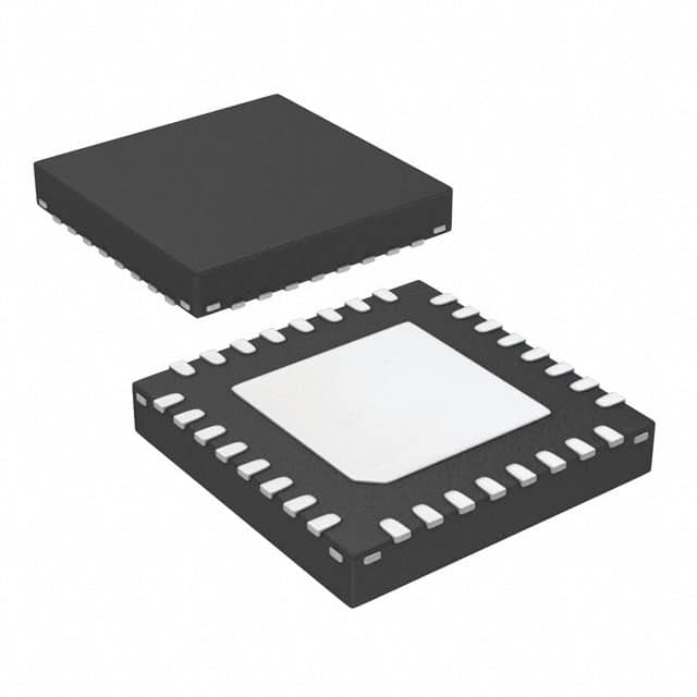
- Part No.:
- LE79R79-1FQC
- Manufacturer:
- Microchip Technology
- Category:
- Telecom
- Package:
- 32-VQFN Exposed Pad
- Datasheet:
-
 LE79R79-1FQC.pdf
- Description:
- IC TELECOM INTERFACE 32QFN
- Quantity:
- Payment:

- Shipping:

Inventory:2,901
Please send an inquiry. Send us your inquiry, and we will respond immediately.
Product details
Overview
LE79R79-1FQC from Zarlink Semiconductor is a bipolar monolithic Ringing Subscriber Line Interface Circuit (R-SLIC) designed for short-loop telephony CPE applications. It integrates on-chip trapezoidal ringing, programmable constant-current feed (IL = 20–39 mA), on-hook transmission (OHT), and dual battery switching (VBAT1: –40.5 to –75 V; VBAT2: –19 V to VBAT1). It delivers 66–69 Vpk ringing output into 1570 Ω and supports ISDN-TA, DSL modems, and smart residential gateways.
For engineers reviewing the LE79R79-1FQC datasheet, LE79R79-1FQC pinout, LE79R79-1FQC application, or LE79R79-1FQC equivalent, key selection criteria include longitudinal balance (52 dB, normal polarity), integrated ring-trip detection, ground-key/loop-detect threshold programmability, and QFN-32 green RoHS-compliant packaging with exposed thermal pad tied to VBAT1.
Technical Context
The LE79R79-1FQC implements full BORSHT functionality-battery feed, overvoltage protection, ringing, supervision, hybrid, and test-with on-chip trapezoidal ringing generation via CMOS-compatible RINGIN input and external RC shaping network. Its dual-battery architecture switches between VBAT1 (high-voltage standby) and VBAT2 (low-voltage active) to meet LSSGR five-ringer voltage requirements while minimizing power dissipation in off-hook states.
It features a 1000× current gain at RSN node for precise loop-current sensing, programmable open-circuit voltage via RSGH/RSGL resistors, and two open-collector relay drivers (RYOUT1/RYOUT2) with built-in 15 kΩ pull-up on DET output. Supervision includes polarity reversal option (enabled by -1 suffix), ground-key detection, and tip-open capability for ground-start signaling.
Key Specifications
| Parameter | Value and Actual Design Meaning |
|---|---|
| Ring Output Voltage | 66–69 Vpk into 1570 Ω load; meets LSSGR five-ringer spec under VBAT1 = −75 V. |
| Longitudinal Balance | 52 dB (normal polarity); enables compliance with CCITT G.712 and LSSGR noise rejection requirements. |
| Constant-Current Feed Range | 20–39 mA; programmable via RDC network; supports long-loop (RLDC = 750 Ω) and short-loop operation. |
| Battery Supply Range | VBAT1: −40.5 to −75 V; VBAT2: −19 V to VBAT1; enables low-power active mode and high-voltage standby. |
| Power Dissipation (QFN) | 3.00 W max at TA = 70°C; enabled by thermally enhanced QFN-32 package with exposed VBAT1-tied pad. |
| Loop-Detect Threshold Accuracy | ±20% in active state; set via RD resistor (min 56 kΩ); supports reliable off-hook/on-hook state detection. |
| THD (Active State) | −50 to −64 dB at +3 dBm, VBAT2 = −24 V; ensures clean voice path for VoIP and analog telephony interfaces. |
Pinout & Package
LE79R79-1FQC uses a 32-pin QFN package with exposed thermal pad electrically connected to VBAT1. The package is green (RoHS-compliant), halogen-free, and lead-free, with matte-tin plating compatible with lead-free reflow profiles (peak ≤ 245°C).
| Pin/Terminal | Circuit Role | Design Meaning |
|---|---|---|
| A(TIP) | Output amplifier terminal | Drives TIP line; metallic AC/DC voltage referenced to BGND; supports 150 mA peak current. |
| B(RING) | Output amplifier terminal | Drives RING line; symmetric to A(TIP); enables two-wire interface with programmable impedance. |
| RSN | Receive summing node | 1000× current gain node; connects DC-feed, receive gain, and two-wire impedance networks. |
| RINGIN | Digital ringing input | CMOS-compatible square-wave input; shaped externally to trapezoidal waveform for ringing generation. |
| RYOUT1 / RYOUT2 | Open-collector relay drivers | Drive external relays; RYE is common emitter; each supports 75 mA sink current. |
| VBAT1 / VBAT2 | Battery supplies | VBAT1 powers standby/high-voltage modes; VBAT2 powers active/low-power modes; B2EN selects source. |
| RTRIP1 / RTRIP2 | Ring-trip detector inputs | Set ring-trip threshold and offset; RTRIP2 enables VBAT1 switch during non-ringing states for power conservation. |
| DET | Hook-switch detector output | Open-collector logic-low output indicating tripped detector; internal 15 kΩ pull-up to VCC. |
Key Features
| Feature | Design Value |
|---|---|
| On-chip trapezoidal ringing | Eliminates external ringing transformer; reduces BOM cost and board area in ISDN-TA and DSL modem designs. |
| Programmable open-circuit voltage | Set via RSGH resistor; ensures compatibility with fax machines and MTUs requiring ≥42.8 V OCV. |
| Two-battery feed architecture | Switches between VBAT1 (standby) and VBAT2 (active); cuts standby power by >50% vs single-battery SLICs. |
| Integrated ring-trip detector | Monitors line current during ringing; triggers DET output to signal ring termination without external circuitry. |
| Ground-key and loop-detect thresholds | Independently programmable via RD and RTRIP1; supports diverse CPE hook-switch and ground-start implementations. |
| Internal VEE regulator | Generates −5 V from VNEG; removes need for external negative supply, simplifying power design. |
Applications
| ISDN Terminal Adaptor (TA) | DSL Modem |
|---|---|
Use Scenario: Provides analog telephone interface for ISDN-to-PSTN bridging in home/office TA units. IC Role / Device Role / Timing Role: Full BORSHT SLIC handling battery feed, ringing, supervision, and hybrid functions. Use Value: On-chip trapezoidal ringing eliminates external transformer; 52 dB longitudinal balance ensures low crosstalk in multi-line TA chassis. | Use Scenario: Enables POTS port integration in ADSL/VDSL modems for legacy phone service backup. IC Role / Device Role / Timing Role: Two-wire line driver with programmable impedance and OHT capability for voice channel separation. Use Value: Dual-battery switching reduces standby power to <100 mW; meets Energy Star and EU ErP Lot 6 requirements. |
| Smart Residential Gateway | Cable Modem with VoIP |
Use Scenario: Delivers PSTN line interface in converged gateways supporting VoIP, Wi-Fi, and Ethernet. IC Role / Device Role / Timing Role: Ringing SLIC with relay drivers for FXS port control and line seizure management. Use Value: RYOUT1/RYOUT2 drive external relays for line isolation; polarity reversal (-1 suffix) supports global telco signaling variants. | Use Scenario: Adds analog telephony support to DOCSIS cable modems for triple-play service delivery. IC Role / Device Role / Timing Role: SLIC with integrated ring-trip detection and programmable loop-detect threshold for reliable call progress monitoring. Use Value: ±20% loop-detect accuracy ensures robust off-hook detection across temperature (−40 to +85°C) and line resistance variations. |
Equivalent & Alternatives
The following parts are listed as comparable options for similar ringing SLIC applications.
| Alternative Part | Technical Difference | Application Difference | Selection Advice |
|---|---|---|---|
| LE79R79-2FQC | 63 dB longitudinal balance (reverse polarity); higher noise rejection than LE79R79-1FQC's 52 dB. | Preferred for ETSI-compliant deployments requiring stricter longitudinal noise suppression. | Select when system-level longitudinal balance must exceed 52 dB; same pinout and firmware interface. |
| LE79R100-1FQC | Higher ring voltage (75 Vpk), wider VBAT1 range (−36 to −90 V), and integrated DC-DC converter for VNEG generation. | Suitable for longer loops and legacy central office environments where higher ringing energy is mandated. | Choose for extended reach or future-proofing; requires minor layout changes due to different RDC/RSN biasing. |
Compared with LE79R79-2FQC, LE79R79-1FQC offers lower-cost compliance for North American LSSGR applications; compared with LE79R100-1FQC, it provides optimized power efficiency and smaller footprint for short-loop CPE where 69 Vpk suffices.
Availability
LE79R79-1FQC is available at Aetrix Electronics and suitable for ISDN-TA, DSL modems, smart residential gateways, and cable modems requiring stable component supply, RoHS-compliant green packaging, and industrial temperature support (−40 to +85°C).
Supply support for LE79R79-1FQC includes scheduled delivery planning, volume procurement assistance, BOM continuity management, traceable sourcing, and lifecycle availability coordination for OEM customers, industrial embedded developers, connected-device designers, and electronics production programs.
Manufacturer
Zarlink Semiconductor was a fabless IC designer specializing in communications semiconductors, later acquired by Microsemi (now Microchip Technology). It pioneered high-integration SLIC solutions for telecom infrastructure and CPE.
The VE580 Series-including LE79R79-1FQC-was engineered for cost-sensitive, space-constrained short-loop telephony endpoints, emphasizing on-chip ringing, dual-battery efficiency, and programmable supervision to replace discrete SLIC+ringing transformer designs.
FAQ
What is the primary function of the LE79R79-1FQC in a telephony system?
The LE79R79-1FQC serves as a Ringing Subscriber Line Interface Circuit (R-SLIC), providing full BORSHT functionality-including battery feed, ringing generation, supervision, and hybrid functions-for analog telephone line interfaces. In systems like DSL modems or ISDN terminal adaptors, the LE79R79-1FQC replaces discrete SLIC and external ringing transformers by integrating trapezoidal ringing, dual-battery switching, and programmable loop-current feed on a single monolithic bipolar IC.
How does the LE79R79-1FQC achieve power savings in standby mode?
The LE79R79-1FQC achieves standby power savings through its dual-battery architecture: it automatically switches from high-voltage VBAT1 (−40.5 to −75 V) in on-hook/open-circuit states to low-voltage VBAT2 (−19 V to VBAT1) in off-hook/active states. This reduces quiescent power consumption to just 48–100 mW in standby, versus >200 mW for single-supply SLICs-critical for Energy Star–compliant residential gateways. The B2EN pin controls this switching, and RTRIP2 enables VBAT1 re-engagement during non-ringing intervals.
What does the "-1" in LE79R79-1FQC indicate, and how does it affect performance?
The "-1" in LE79R79-1FQC denotes the performance grade: 52 dB longitudinal balance in normal polarity configuration. This grade meets LSSGR and FCC Part 68 requirements for North American short-loop CPE but does not support polarity reversal (unlike -2 grade). The "-1" suffix also confirms RoHS-compliant green packaging and QFN-32 tray delivery. Systems requiring ETSI-compliant 63 dB balance or polarity reversal must use LE79R79-2FQC instead.
Can the LE79R79-1FQC drive standard telephone ringers without external components?
Yes-the LE79R79-1FQC can drive standard telephone ringers directly using its integrated trapezoidal ringing generator. It delivers 66–69 Vpk into a 1570 Ω load (equivalent to five ringer equivalents per LSSGR), conditioned by a CMOS-compatible RINGIN square wave and an external RC shaping network. No external transformer or high-voltage amplifier is needed. However, RINGIN must be driven with 50% duty-cycle CMOS logic, and the RC network must be sized per the LE79R79 User's Guide (Doc #080914) to meet spectral mask requirements.
What thermal considerations apply to the LE79R79-1FQC in QFN-32 package?
The LE79R79-1FQC in QFN-32 relies on its exposed thermal pad-electrically connected to VBAT1-for heat dissipation. To achieve the specified 3.00 W max power dissipation at TA = 70°C, the pad must be soldered to an equally sized copper pour on the PCB, connected via ≥4 thermal vias to an internal ground or VBAT1 plane. Failure to implement this degrades θJA from 25°C/W to >40°C/W, risking thermal shutdown above 145°C junction temperature. The datasheet mandates IPC/JEDEC J-Std-020B reflow profile compliance.
LE79R79-1FQC Specifications
- Product attributes
- Attribute value
- Manufacturer:
- Microchip Technology
- Series:
- -
- Package/Case:
- 32-VQFN Exposed Pad
- Packaging:
- Tray
- Product Status:
- Obsolete
- Function:
- Subscriber Line Interface Concept (SLIC)
- Interface:
- 2-Wire
- Number of Circuits:
- 1
- Voltage - Supply:
- 4.75V ~ 5.25V
- Current - Supply:
- -
- Power (Watts):
- -
- Operating Temperature:
- 0°C ~ 70°C
- Grade:
- -
- Qualification:
- -
- Mounting Type:
- Surface Mount
- Supplier Device Package:
- 32-QFN (8x8)
LE79R79-1FQC FAQ
1.How can I place an order for LE79R79-1FQC through Aetrix?
Please submit a Request for Quotation (RFQ) for LE79R79-1FQC on Aetrix. Our sales agent will provide a competitive quotation and guide you through the order confirmation once you accept the terms.
2.Are the price and stock information for LE79R79-1FQC reliable?
The price and inventory of LE79R79-1FQC are updated periodically and may fluctuate due to market conditions. Stock and pricing data are typically refreshed every 24 hours. Quotation validity for LE79R79-1FQC is usually 5 days.
3.What payment methods are accepted for LE79R79-1FQC?
We accept Wire Transfer, PayPal, Credit Card, Western Union, MoneyGram, and Escrow for LE79R79-1FQC transactions.
Note: Certain payment methods may incur a processing fee.
4.How is shipping managed for LE79R79-1FQC?
LE79R79-1FQC orders can be shipped via leading logistics carriers, including DHL, UPS, FedEx, TNT, or Registered Mail.
Once your LE79R79-1FQC order is processed, you will receive an email with the shipment details and tracking number.
Note: Tracking information may take up to 24 hours to appear. Express delivery typically takes 3–5 business days.
5.How can I obtain technical support or documentation for LE79R79-1FQC?
For technical support, including LE79R79-1FQC datasheets, pinout diagrams, or application guidance, please contact our engineering support team. They can provide detailed documentation and assistance for your LE79R79-1FQC requirements.
6.How does Aetrix verify that LE79R79-1FQC is sourced from the original manufacturer or authorized distributors?
All LE79R79-1FQC products on Aetrix are procured from qualified distributors and authorized channels. Our dedicated quality assurance team conducts strict verification, including traceability checks and, if necessary, third-party testing. This ensures that LE79R79-1FQC meets industry standards.
7.What is the process for return or replacement of LE79R79-1FQC?
All LE79R79-1FQC units undergo pre-shipment inspection (PSI). If there is an issue with LE79R79-1FQC, returns or replacements are accepted under the following conditions:
1.Quantity discrepancies, incorrect items, or visible external defects (such as breakage or corrosion), acknowledged by Aetrix.
2.The issue is reported within 90 days of delivery.
3.The LE79R79-1FQC part is unused and in its original packaging.
Return procedure for LE79R79-1FQC:
1.Submit a request within 90 days.
2.Obtain a Return Material Authorization (RMA) from Aetrix.
LE79R79-1FQC Tags

-
LMC567CMX/NOPB
Texas Instruments
-
LM567CMX/NOPB
Texas Instruments
-
LM567CM/NOPB
Texas Instruments

-
VSC8531XMW-02
Microchip Technology
-
VSC8531XMW-05
Microchip Technology

-
GPY115C0VI
MaxLinear, Inc.

-
SI32185-A-FMR
Skyworks Solutions Inc.

-
VSC8541XMV-05
Microchip Technology

-
SI32178-B-FM1R
Skyworks Solutions Inc.
-
GPY215C0VI
MaxLinear, Inc.

-
CPC7514ZTR
Littelfuse Inc.

-
VSC8502XML-03
Microchip Technology
Tech Hub

TTL and CMOS logic families differ in thresholds, loading, output drive, power and timing. This engineering guide compares 74HC and 74HCT, calculates noise margins and checks 3.3 V/5 V compatibility.

A practical engineering guide to 3.3V and 5V logic compatibility, input thresholds, resistor dividers, translator ICs, MOSFET level shifting, I2C pull-ups, timing limits and power-sequencing risks.

The 74HC595 uses push-pull logic outputs, while the TPIC6B595 uses 50 V open-drain DMOS sinks for higher-power loads. This guide compares timing, current limits, 3.3 V interfacing, load wiring, thermal…

The 74HC595 converts serial data into eight stable parallel outputs. This guide covers pin functions, shift and storage timing, OE and MR behavior, drive-current limits, cascading, voltage compatibilit…

A technical comparison of level-sensitive latches and edge-triggered flip-flops, covering timing windows, setup and hold limits, master–slave operation, time borrowing, race-through, HDL inference and…

A D latch stores one bit while Enable controls when data can pass. This reference covers gate-level operation, truth tables, transparency, setup and hold timing, LE versus OE, common ICs and practical …

An SR latch stores one bit through cross-coupled feedback. This engineering reference covers NOR and NAND implementations, truth tables, forbidden-state recovery, gated operation, switch debouncing, fa…

Latch circuits retain one bit through feedback. This technical reference covers SR and D latches, truth tables, transparency, timing limits, latch-versus-flip-flop behavior, applications and common log…

An engineering guide to LED driver operation, constant-current and constant-voltage outputs, linear and switching topologies, dimming, IC selection, calculations, replacement compatibility, and fault c…

Operational amplifier guide covering op amp basics, feedback, ideal vs real op amps, common configurations, buffer circuits, offset, bias current, gain-bandwidth, slew rate, rail-to-rail limits and sel…


