
 My Inquiry
 My Account


Texas Instruments LM2512ASN/NOPB
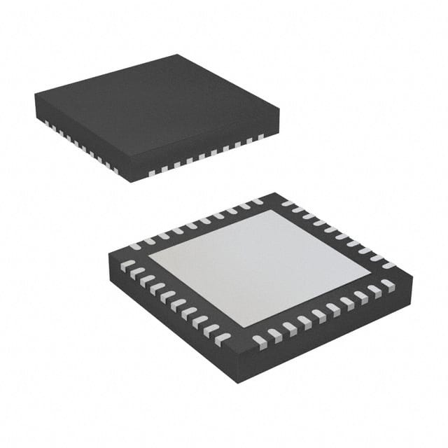
- Part No.:
- LM2512ASN/NOPB
- Manufacturer:
- Texas Instruments
- Category:
- Serializers, Deserializers
- Package:
- 48-XFQFN Exposed Pad
- Datasheet:
-
 LM2512ASN/NOPB.pdf
- Description:
- IC MPL1 SERIALIZER 24BIT 40X2QFN
- Quantity:
- Payment:

- Shipping:

Inventory:4,214
Please send an inquiry. Send us your inquiry, and we will respond immediately.
Product details
Overview
LM2512ASN/NOPB from Texas Instruments is a Mobile Pixel Link (MPL-1) Serializer IC that converts 24-bit RGB + VS/HS/DE video signals into a 2- or 3-lane MPL serial stream. It supports up to 640×480 VGA at 22.5 MHz PCLK, performs optional 24-to-18-bit stochastic dithering, and integrates a three-channel 256×8-bit LUT for independent color correction. It operates with 1.6–2.0 V core/analog supply and 1.6–3.0 V I/O supply.
For engineers reviewing the LM2512ASN/NOPB datasheet, LM2512ASN/NOPB pinout, LM2512ASN/NOPB application, or LM2512ASN/NOPB equivalent, key selection criteria include MPL-1 physical layer compliance, dithering algorithm fidelity, SPI-configurable lane count (2 vs 3 MD), LUT enable/disable behavior across power-down cycles, and current-mode MPL driver output specifications (IB = 190 µA, IOLL/IOLH ratios).
Technical Context
The LM2512ASN/NOPB implements an MPL Level 0 Enhanced Protocol with Class 0 PHY, using single-ended current-mode signaling on MD[2:0] and MC lines. Its PLL locks to PCLK (5–22.5 MHz), generating an 80 MHz MC clock at 20 MHz PCLK in 3-lane mode, enabling 160 Mbps per MD lane (480 Mbps raw throughput).
It features dual-phase startup: bias block activation (t₀ = 200 PCLK cycles), followed by MC-driven link-up sequence (t₁–t₄) including current-level calibration and PLL lock (600-cycle hold-off). Frame synchronization uses auto-resync via F[1:0] incrementing bits embedded in every pixel payload.
Key Specifications
| Parameter | Value and Actual Design Meaning |
|---|---|
| PCLK Range | 5–22.5 MHz (supports QVGA to VGA; 3-lane: 7.5–22.5 MHz, 2-lane: 5–15 MHz) |
| MPL Output Type | Single-ended current-mode drivers (IB = 190 µA; IOLL = 5×IB, IOLH = 1×IB) |
| Dither Resolution | 24-bit → 18-bit stochastic dither with blue-noise characteristic; requires VS input |
| LUT Capacity | Three independent 256×8-bit SRAMs (Red/Green/Blue); disabled by default and after PD* cycle |
| Supply Voltages | VDD/VDDA: 1.6–2.0 V; VDDIO: 1.6–3.0 V; enables level translation between host and display |
| Power-Down Current | <5 µA total (VDD/VDDA + VDDIO) when PD* = L or PCLK stopped |
| SPI Interface | 3-wire (CSX/SCL/SDA); supports 16-bit WRITE/READ and PAGE WRITE; requires REG22 unlock |
Pinout & Package
LM2512ASN/NOPB is packaged in a 40-pin QFN (NJM0040A) with 0.5 mm pitch and exposed thermal pad (VSSIO). Pin functions are validated per TI SNLS269B Rev. May 2013.
| Pin/Terminal | Circuit Role | Design Meaning |
|---|---|---|
| R[7:0], G[7:0], B[7:0] | Parallel RGB data inputs | 24-bit LVCMOS video bus; latched on PCLK rising edge; MSB-aligned for dither bypass |
| VS, HS, DE, PCLK | Video timing control inputs | LVCMOS synchronous interface; VS required for dither frame alignment; DE polarity configurable via register |
| MD[2:0], MC | MPL serial output drivers | Current-mode outputs (3 MD lanes + clock); support 2-lane (default) or 3-lane configuration via SPI |
| SPI_CSX, SPI_SCL, SPI_SDA/HS | SPI configuration interface | Multi-function: SDA doubles as HS input when CSX high; SPI disabled during PD* = L or PCLK stop |
| PD* | Active-high enable input | Drives SER into sleep mode (<5 µA) when low; resets registers but retains LUT data |
| VDDA, VDD, VDDIO, VSSA, VSS, VSSIO | Power and ground rails | Separate analog (VDDA/VSSA), core (VDD/VSS), and I/O (VDDIO/VSSIO) domains for noise isolation |
Key Features
| Feature | Design Value |
|---|---|
| 24-bit to 18-bit dithering | Stochastic "blue noise" algorithm minimizes visible patterning; frame-aligned using VS signal |
| Configurable MPL lane count | SPI-selectable 2-lane (default) or 3-lane operation; adjusts raw throughput from 320 to 480 Mbps |
| Independent color correction | Three 256×8-bit LUTs (R/G/B) loaded via SPI; retained across PD* cycles but lost on full power loss |
| Intrinsic level translation | Accepts 1.6–3.0 V LVCMOS inputs while driving MPL current-mode outputs referenced to 1.6–2.0 V |
| Auto-resync frame sequencing | F[1:0] bits auto-increment per pixel; enables deserializer to detect and recover from sync loss without overhead coding |
| Low-power link management | Power-down current <5 µA; supports STOP-PCLK auto-power-down and PD*-controlled sleep entry/exit |
Applications
| Mobile Display Interconnect | VGA Resolution Video Bridge |
|---|---|
Use Scenario: Connecting baseband or graphics processor to thin-film transistor (TFT) LCD panel in smartphones or portable media players. IC Role / Device Role / Timing Role: Serializer translating parallel 24-bit RGB bus to compact 3-signal MPL interface, reducing flex cable count from 28 to 4 lines. Use Value: Enables high-resolution (640×480) display transmission with <5 µA standby current and intrinsic 1.6–3.0 V level translation. |
Use Scenario: Replacing legacy parallel RGB interfaces in industrial VGA monitors where EMI and board space are constrained. IC Role / Device Role / Timing Role: MPL serializer supporting 22.5 MHz PCLK for 60 Hz VGA timing, with dithering preserving perceived color depth on 18-bit panels. Use Value: Eliminates external termination and reduces interconnect EMI via current-mode MPL signaling compliant with 50–100 Ω microstrip/stripline traces. |
| Color-Calibrated Display Module | Low-Power Embedded Display Link |
Use Scenario: Integrating factory-calibrated gamma and white-point correction into automotive instrument clusters or medical displays. IC Role / Device Role / Timing Role: Configurable LUT applying per-channel 8-bit lookup to RGB data pre-serialization; loaded once at boot via SPI. Use Value: Achieves precise color matching without host CPU intervention; LUT contents retained across PD* cycles for instant wake-up fidelity. |
Use Scenario: Power-sensitive wearable devices requiring display updates only during user interaction. IC Role / Device Role / Timing Role: Serializer entering sub-5 µA sleep state when PD* is pulled low or PCLK halted, with full restart in <1 ms after wake. Use Value: Extends battery life via hardware-managed low-power states-no firmware coordination needed for link shutdown/restart. |
Equivalent & Alternatives
The following parts are listed as comparable options for similar MPL serializer applications.
| Alternative Part | Technical Difference | Application Difference | Selection Advice |
|---|---|---|---|
| LM2511ASN/NOPB | No dithering engine; no LUT; fixed 2-lane MPL only; lower ICC (4.1 mA typical) | Suitable only for 18-bit-native sources; lacks color correction and frame-sync resiliency | Select when cost and power are critical and dithering/LUT are unnecessary |
| DS90C124MTD/NOPB | FPD-Link II serializer (not MPL); 24-bit RGB + control; LVDS outputs; higher voltage (3.3 V) | Requires matched-pair differential routing; incompatible with MPL deserializers like FPD95320 | Choose only when migrating existing FPD-Link II infrastructure; not drop-in for MPL systems |
Compared with LM2512ASN/NOPB, LM2511ASN/NOPB removes dithering and LUT to reduce cost and active current, while DS90C124MTD/NOPB replaces MPL's current-mode simplicity with LVDS complexity and higher system-level routing demands.
Availability
LM2512ASN/NOPB is available at Aetrix Electronics and suitable for mobile display interconnect, VGA resolution video bridge, color-calibrated display module, and low-power embedded display link applications requiring stable component supply and long-term lifecycle support.
Supply support for LM2512ASN/NOPB includes scheduled delivery planning, volume procurement assistance, BOM continuity management, traceable sourcing, and lifecycle availability coordination for OEM customers, industrial embedded developers, connected-device designers, and electronics production programs.
Manufacturer
Texas Instruments is a global semiconductor company specializing in analog, embedded processing, and connectivity technologies with over 50 years of leadership in high-reliability interface solutions.
The LM2512ASN/NOPB belongs to TI's Mobile Pixel Link (MPL) interface product line, designed specifically to replace bulky parallel RGB buses in space- and power-constrained portable displays while maintaining visual fidelity through dithering and color correction.
FAQ
What is the maximum PCLK frequency supported by the LM2512ASN/NOPB in 3-lane mode?
The LM2512ASN/NOPB supports up to 22.5 MHz PCLK in 3-lane mode, enabling full 640×480 VGA at 60 Hz. At this rate, the internal PLL generates an 80 MHz MC clock, delivering 160 Mbps per MD lane for 480 Mbps raw throughput. Operation above 22.5 MHz violates the recommended operating conditions and risks timing violations in the dither block and MPL serialization logic.
Does the LM2512ASN/NOPB retain LUT data during power-down mode?
Yes, the LM2512ASN/NOPB retains LUT SRAM contents when entering power-down mode via PD* = L or PCLK stop. However, LUT functionality remains disabled until explicitly re-enabled via SPI register write (REG0 = 01h) after wake-up. Full power cycling (VDD/VDDA removal) clears LUT data, requiring reload before use.
Can the LM2512ASN/NOPB operate with a 1.2 V I/O supply?
No, the LM2512ASN/NOPB requires VDDIO between 1.6 V and 3.0 V per its absolute maximum and recommended operating conditions. A 1.2 V supply falls outside specification and will result in undefined LVCMOS input thresholds (VIH/VIL), unreliable SPI communication, and potential failure of the R/G/B input buffers. Minimum valid VDDIO is 1.6 V.
How does the LM2512ASN/NOPB handle synchronization loss on the MPL link?
The LM2512ASN/NOPB embeds auto-incrementing F[1:0] frame sequence bits in every pixel payload. When synchronization is lost, the companion deserializer detects the repeating 2-bit pattern and realigns the data stream without protocol overhead or pixel expansion. This method adds only 3/24 = 12.5% overhead per pixel and requires no host intervention.
Is the LM2512ASN/NOPB pin-compatible with the LM2512A without the /NOPB suffix?
Yes, LM2512ASN/NOPB is the RoHS-compliant, lead-free packaging variant of the LM2512A. Both share identical pinout, electrical characteristics, timing, and functional behavior. The /NOPB suffix denotes green packaging (Pb-free, halogen-free) and does not affect circuit design, layout, or firmware compatibility.
LM2512ASN/NOPB Specifications
- Product attributes
- Attribute value
- Manufacturer:
- Texas Instruments
- Series:
- -
- Package/Case:
- 48-XFQFN Exposed Pad
- Packaging:
- Tape & Reel (TR)
- Product Status:
- Obsolete
- Function:
- Serializer
- Data Rate:
- 468Mbps
- Input Type:
- LVCMOS
- Output Type:
- MPL
- Number of Inputs:
- 28
- Number of Outputs:
- 3
- Voltage - Supply:
- 1.6V ~ 3V
- Operating Temperature:
- -30°C ~ 85°C (TA)
- Grade:
- -
- Qualification:
- -
- Mounting Type:
- Surface Mount
- Supplier Device Package:
- 40-X2QFN (6x6)
LM2512ASN/NOPB FAQ
1.How can I place an order for LM2512ASN/NOPB through Aetrix?
Please submit a Request for Quotation (RFQ) for LM2512ASN/NOPB on Aetrix. Our sales agent will provide a competitive quotation and guide you through the order confirmation once you accept the terms.
2.Are the price and stock information for LM2512ASN/NOPB reliable?
The price and inventory of LM2512ASN/NOPB are updated periodically and may fluctuate due to market conditions. Stock and pricing data are typically refreshed every 24 hours. Quotation validity for LM2512ASN/NOPB is usually 5 days.
3.What payment methods are accepted for LM2512ASN/NOPB?
We accept Wire Transfer, PayPal, Credit Card, Western Union, MoneyGram, and Escrow for LM2512ASN/NOPB transactions.
Note: Certain payment methods may incur a processing fee.
4.How is shipping managed for LM2512ASN/NOPB?
LM2512ASN/NOPB orders can be shipped via leading logistics carriers, including DHL, UPS, FedEx, TNT, or Registered Mail.
Once your LM2512ASN/NOPB order is processed, you will receive an email with the shipment details and tracking number.
Note: Tracking information may take up to 24 hours to appear. Express delivery typically takes 3–5 business days.
5.How can I obtain technical support or documentation for LM2512ASN/NOPB?
For technical support, including LM2512ASN/NOPB datasheets, pinout diagrams, or application guidance, please contact our engineering support team. They can provide detailed documentation and assistance for your LM2512ASN/NOPB requirements.
6.How does Aetrix verify that LM2512ASN/NOPB is sourced from the original manufacturer or authorized distributors?
All LM2512ASN/NOPB products on Aetrix are procured from qualified distributors and authorized channels. Our dedicated quality assurance team conducts strict verification, including traceability checks and, if necessary, third-party testing. This ensures that LM2512ASN/NOPB meets industry standards.
7.What is the process for return or replacement of LM2512ASN/NOPB?
All LM2512ASN/NOPB units undergo pre-shipment inspection (PSI). If there is an issue with LM2512ASN/NOPB, returns or replacements are accepted under the following conditions:
1.Quantity discrepancies, incorrect items, or visible external defects (such as breakage or corrosion), acknowledged by Aetrix.
2.The issue is reported within 90 days of delivery.
3.The LM2512ASN/NOPB part is unused and in its original packaging.
Return procedure for LM2512ASN/NOPB:
1.Submit a request within 90 days.
2.Obtain a Return Material Authorization (RMA) from Aetrix.
LM2512ASN/NOPB Tags

-
SN65HVS880PWPR
Texas Instruments
-
SN65HVS882PWPR
Texas Instruments

-
FIN3386MTDX
onsemi
-
FIN3385MTDX
onsemi

-
SN65LV1023ARHBR
Texas Instruments

-
SN65LV1023ADBR
Texas Instruments
-
SN65LV1224BDBR
Texas Instruments

-
SN65LVDS93ADGGR
Texas Instruments
-
SN65LVDS93DGGR
Texas Instruments

-
TDES954RGZT
Texas Instruments
-
SN65LV1224BRHBT
Texas Instruments

-
DS90UB914QSQE/NOPB
Texas Instruments
Tech Hub

A practical engineering guide to 3.3V and 5V logic compatibility, input thresholds, resistor dividers, translator ICs, MOSFET level shifting, I2C pull-ups, timing limits and power-sequencing risks.

The 74HC595 uses push-pull logic outputs, while the TPIC6B595 uses 50 V open-drain DMOS sinks for higher-power loads. This guide compares timing, current limits, 3.3 V interfacing, load wiring, thermal…

The 74HC595 converts serial data into eight stable parallel outputs. This guide covers pin functions, shift and storage timing, OE and MR behavior, drive-current limits, cascading, voltage compatibilit…

A technical comparison of level-sensitive latches and edge-triggered flip-flops, covering timing windows, setup and hold limits, master–slave operation, time borrowing, race-through, HDL inference and…

A D latch stores one bit while Enable controls when data can pass. This reference covers gate-level operation, truth tables, transparency, setup and hold timing, LE versus OE, common ICs and practical …

An SR latch stores one bit through cross-coupled feedback. This engineering reference covers NOR and NAND implementations, truth tables, forbidden-state recovery, gated operation, switch debouncing, fa…

Latch circuits retain one bit through feedback. This technical reference covers SR and D latches, truth tables, transparency, timing limits, latch-versus-flip-flop behavior, applications and common log…

An engineering guide to LED driver operation, constant-current and constant-voltage outputs, linear and switching topologies, dimming, IC selection, calculations, replacement compatibility, and fault c…

Operational amplifier guide covering op amp basics, feedback, ideal vs real op amps, common configurations, buffer circuits, offset, bias current, gain-bandwidth, slew rate, rail-to-rail limits and sel…

Jumper cables guide covering safe connection order, red and black clamp placement, final ground connection, cable gauge, length, clamp quality, copper vs CCA cables, jump starter comparison and battery…


