
 My Inquiry
 My Account


Texas Instruments LM27965SQ-M/NOPB
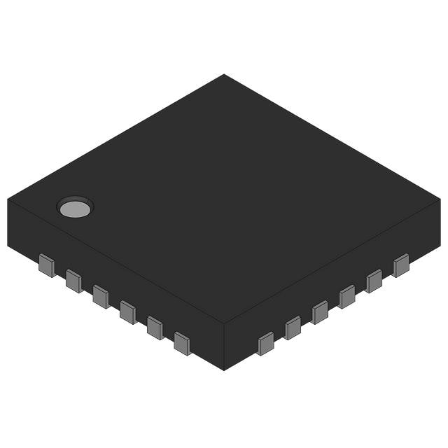
- Part No.:
- LM27965SQ-M/NOPB
- Manufacturer:
- Texas Instruments
- Category:
- LED Drivers
- Package:
- 24-WFQFN Exposed Pad
- Datasheet:
-
 LM27965SQ-M/NOPB.pdf
- Description:
- IC LED DRV RGLTR I2C 30MA 24WQFN
- Quantity:
- Payment:

- Shipping:

Inventory:1,930
Please send an inquiry. Send us your inquiry, and we will respond immediately.
Product details
Overview
LM27965SQ-M/NOPB from Texas Instruments is a dual-display white LED driver IC with I²C-compatible brightness control, adaptive 1×/3/2× charge pump, and three independently controlled current-sink banks (BankA: up to 5 LEDs, BankB: up to 3 LEDs, BankC: 1 indicator LED). It delivers up to 180mA total output current, achieves 91% peak efficiency, and supports 2.7V–5.5V input for mobile phone and PDA display lighting.
For engineers reviewing the LM27965SQ-M/NOPB datasheet, LM27965SQ-M/NOPB pinout, LM27965SQ-M/NOPB application, or LM27965SQ-M/NOPB equivalent, this page provides verified technical context, validated pin functions, confirmed I²C address (0x38), exact current-matching specs (0.3% typ.), and real-world design meaning of headroom voltage, gain transition, and PWM-analog hybrid dimming.
Technical Context
The LM27965SQ-M/NOPB implements an adaptive CMOS charge pump that dynamically switches between 1× pass-through and 3/2× boost modes based on real-time forward-voltage monitoring of active DxA/DxB pins - triggering at 175mV headroom threshold to maintain regulation. Its internal current sinks use precision 1.25V reference and 200× scaling from ISET to deliver tightly matched LED current across banks.
It integrates three independent brightness control domains: BankA and BankB support 32-step I²C-programmable dimming via combined analog scaling and 20kHz PWM; BankC offers 4-level analog-only control. The device uses dedicated VIO pin for I²C logic level translation and includes hardware RESET pin with 0.45V threshold for system-level fault recovery.
Key Specifications
| Parameter | Value and Actual Design Meaning |
|---|---|
| Input Voltage Range | 2.7V to 5.5V - supports single-cell Li-ion battery operation without external LDO. |
| Total Output Current | 180mA max - distributable across BankA (≤125mA), BankB (≤45mA), BankC (≤30mA) with per-pin limit of 30mA. |
| LED Current Matching | 0.3% typical - ensures uniform brightness across all LEDs in same bank under varying VIN and temperature. |
| I²C Address | 0x38 (hex) - fixed slave address for LM27965SQ-M variant; enables multi-device bus configuration without address conflict. |
| Charge Pump Gain Modes | Adaptive 1× or 3/2× - automatically selects mode based on VDxx headroom to maximize efficiency across input/LED voltage combinations. |
| Current Setting Accuracy | ±9.5% (BankA/B), ±7.7% (BankC) - guaranteed over full operating temperature range (-30°C to +100°C junction). |
| Startup Time | 250µs - time for POUT to reach 90% steady-state voltage; critical for fast-display wake-up sequences. |
Pinout & Package
LM27965SQ-M/NOPB is housed in a 24-pin WQFN package (4mm × 4mm × 0.8mm, RTW0024A), thermally enhanced with exposed DAP connected to GND for PCB heat dissipation. Pin pitch is 0.5mm; RoHS-compliant and lead-free.
| Pin/Terminal | Circuit Role | Design Meaning |
|---|---|---|
| VIN (24) | Main power input | Accepts 2.7V–5.5V supply; powers charge pump and internal circuitry; requires local 1µF ceramic decoupling. |
| POUT (23) | Charge pump regulated output | Delivers boosted voltage to LED anodes; voltage tracks VIN in 1× mode or = 1.5×VIN in 3/2× mode minus ROUT drop. |
| C1 (19,22), C2 (20,21) | Flying capacitor connections | Interface with internal charge pump switches; requires two 1µF low-ESR MLCCs (e.g., TDK C1608X5R1A105K). |
| D1A–D5A (12–16) | BankA LED cathode drivers | Five independent current sinks for main display; each sinks up to 30mA; forward-voltage sensing enabled by default. |
| D1B–D3B (4–6) | BankB LED cathode drivers | Three independent current sinks for sub-display; each sinks up to 30mA; forward-voltage sensing enabled by default. |
| D1C (3) | Indicator LED driver | Single current sink for status LED; no forward-voltage sensing; supports 4-level analog dimming only. |
| ISET (17) | Current reference programming | Connects to GND via RSET resistor; sets full-scale current as IDxx = 200 × (1.25V / RSET); tolerance directly impacts LED brightness accuracy. |
| SCL (1), SDIO (2) | I²C serial interface | Standard bidirectional I²C bus signals; referenced to VIO; require pull-up resistors to VIO; support 100kHz–400kHz operation. |
| VIO (7) | I²C logic voltage reference | Sets logic threshold for SCL/SDIO; compatible with 1.4V–VIN range; enables interfacing with 1.8V or 3.3V microcontrollers. |
| RESET (10) | Hardware reset input | Active-low asynchronous reset; pulls all registers to power-on defaults when driven ≤0.45V; must be pulled high for normal operation. |
| GND (9,18,DAP) | Ground reference | Three dedicated GND pins plus thermal pad (DAP); all must be connected to solid ground plane for stable regulation and thermal performance. |
| NC (8,11) | No-connect | Internally unconnected; must remain floating or tied to GND per layout guidelines; no electrical function. |
Key Features
| Feature | Design Value |
|---|---|
| Adaptive 1×/3/2× charge pump | Eliminates inductor requirement while maintaining >91% efficiency across 2.7V–5.5V input and 2.0V–4.0V LED Vf range. |
| Three independent LED banks | Enables simultaneous control of main display (BankA), sub-display (BankB), and indicator (BankC) with separate dimming profiles. |
| 0.3% typical current matching | Guarantees consistent luminance across all LEDs in same bank - essential for artifact-free display backlighting. |
| I²C-compatible interface with dual addresses | Supports coexistence of LM27965 (0x36) and LM27965SQ-M/NOPB (0x38) on same bus for multi-display systems. |
| Hardware RESET pin with defined threshold | Provides deterministic power-cycle recovery without firmware dependency; resets all brightness registers and enables to default state. |
Applications
| Mobile Phone Main/Sub Display | PDA Backlight System |
|---|---|
|
Use Scenario: Dual-panel smartphone with high-resolution AMOLED main screen and smaller OLED status bar. IC Role / Device Role / Timing Role: LM27965SQ-M/NOPB drives 5 LEDs in BankA for main display and 3 LEDs in BankB for sub-display, using independent I²C registers for synchronized but distinct brightness curves. Use Value: Achieves uniform luminance across both panels with <0.3% current mismatch, while adaptive gain maintains >88% efficiency at 3.3V input and 3.4V LED Vf. |
Use Scenario: Handheld PDA requiring long battery life and reliable backlight during intermittent use. IC Role / Device Role / Timing Role: LM27965SQ-M/NOPB supplies regulated current to 4 main-display LEDs (BankA) and 2 auxiliary LEDs (BankB), with BankC driving power-status LED. Use Value: 25mm² total solution size and no-inductor design reduce BOM cost and PCB area; shutdown current of 5.4µA extends standby time. |
| Industrial HMI Indicator Lighting | Portable Medical Device Display |
|
Use Scenario: Ruggedized human-machine interface panel with status indicators and segmented LCD backlight. IC Role / Device Role / Timing Role: LM27965SQ-M/NOPB uses BankC (D1C) for red/green status LED and BankB (D1B–D2B) for LCD edge-lit backlight, all controlled via single I²C bus. Use Value: Hardware RESET pin enables fail-safe recovery during ESD events; extended -30°C to +85°C ambient rating ensures operation in harsh environments. |
Use Scenario: Battery-powered ultrasound or glucose monitor with clinical-grade display brightness consistency. IC Role / Device Role / Timing Role: LM27965SQ-M/NOPB drives 5 main-display LEDs (BankA) with 32-step PWM dimming and 1 indicator LED (BankC) for alarm signaling. Use Value: 20kHz PWM frequency avoids audible noise; 0.3% current matching prevents visible banding in grayscale medical images. |
Equivalent & Alternatives
The following parts are listed as comparable options for similar dual-display LED driver applications.
| Alternative Part | Technical Difference | Application Difference | Selection Advice |
|---|---|---|---|
| LM27964SQ/NOPB | Same pinout and package; I²C address 0x36; lacks BankC indicator driver; BankA/B only; 16-level dimming vs. 32-level. | Not suitable for designs requiring independent indicator LED control; limited brightness resolution reduces fine-tuning capability. | Select LM27964SQ/NOPB only if BankC functionality is unused and lower-cost sourcing is prioritized over dimming granularity. |
| TPS61165DRVR | Boost-based (inductor required); single-bank 30mA output; no I²C interface; analog dimming only; no voltage-sensing gain adaptation. | Cannot drive dual displays independently; no hardware RESET; requires external PWM generator for dimming; larger solution size. | Choose TPS61165DRVR only for cost-sensitive single-LED applications where inductor use is acceptable and I²C control is unnecessary. |
Compared with LM27964SQ/NOPB and TPS61165DRVR, LM27965SQ-M/NOPB uniquely combines triple-bank architecture, adaptive charge-pump efficiency, and I²C-address differentiation - enabling compact, low-noise, multi-zone lighting control without layout or firmware redesign.
Availability
LM27965SQ-M/NOPB is available at Aetrix Electronics and suitable for mobile phone display lighting, PDA backlighting, and industrial HMI indicator applications requiring stable component supply, long-term lifecycle support, and traceable sourcing.
Supply support for LM27965SQ-M/NOPB includes scheduled delivery planning, volume procurement assistance, BOM continuity management, traceable sourcing, and lifecycle availability coordination for OEM customers, industrial embedded developers, connected-device designers, and electronics production programs.
Manufacturer
Texas Instruments is a global semiconductor leader specializing in analog, embedded processing, and power management technologies, with decades of expertise in precision LED drivers and portable power solutions.
The LM27965SQ-M/NOPB belongs to TI's white LED driver product line, engineered specifically for space-constrained dual-display devices requiring high-efficiency, no-inductor backlighting with precise current matching and flexible I²C control.
FAQ
What is the I²C slave address for LM27965SQ-M/NOPB?
The LM27965SQ-M/NOPB uses a fixed 7-bit I²C slave address of 0x38 (hex), which corresponds to binary 0111000. This distinguishes it from the standard LM27965 (0x36), allowing both variants to coexist on the same I²C bus without address conflict. The address is hardwired and not software-configurable. All register writes and reads for LM27965SQ-M/NOPB must target 0x38 to ensure proper communication and brightness control.
How does the LM27965SQ-M/NOPB achieve 91% peak efficiency without an inductor?
The LM27965SQ-M/NOPB achieves 91% peak efficiency using an adaptive CMOS charge pump that operates in either 1× pass-through or 3/2× boost mode. When input voltage is sufficient to forward-bias all LEDs, it runs in 1× mode with minimal conduction loss. When VIN drops, it switches to 3/2× mode only as needed - avoiding continuous boost conversion losses. This gain selection, combined with low-RDS(on) internal switches and optimized flying capacitors, eliminates inductor requirements while preserving high efficiency across the 2.7V–5.5V input range.
Can LM27965SQ-M/NOPB drive more than one LED per current sink pin?
Yes - LM27965SQ-M/NOPB supports parallel connection of its DxA or DxB outputs (e.g., D1A–D5A) to drive a single high-current LED. In such configurations, RSET must be selected so that each sink delivers 20% of the desired total current (e.g., 12mA per sink for 60mA total). BankC (D1C) is not designed for parallel use. All Electrical Characteristics - including maximum per-pin current (30mA), headroom voltage, and matching - remain valid in parallel mode, and no internal changes or register settings are required.
What is the role of the VIO pin on LM27965SQ-M/NOPB?
The VIO pin on LM27965SQ-M/NOPB sets the logic reference voltage for the SCL and SDIO I²C interface, supporting 1.4V to VIN levels. It allows direct interfacing with 1.8V or 3.3V microcontrollers without level shifters. Input thresholds scale with VIO: VIH = 0.7×VIO and VIL = 0.3×VIO. Pulling VIO to 1.8V ensures compatibility with low-voltage MCUs while maintaining noise margin; tying VIO to VIN enables 3.3V/5V bus operation. VIO must be externally decoupled with 100nF ceramic capacitor.
How does the RESET pin function on LM27965SQ-M/NOPB?
The RESET pin on LM27965SQ-M/NOPB is an active-low hardware reset input. When driven below 0.45V (typ.), it asynchronously forces all internal registers - including BankA/B/C brightness controls, enable bits, and general-purpose register - to their power-on default states and disables all LED current sinks. During normal operation, RESET must be held high (≥1.2V) via external pull-up. This pin enables robust system-level recovery from brownout or firmware lockup without requiring I²C commands, making LM27965SQ-M/NOPB suitable for safety-critical or field-deployed devices.
LM27965SQ-M/NOPB Specifications
- Product attributes
- Attribute value
- Manufacturer:
- Texas Instruments
- Series:
- -
- Package/Case:
- 24-WFQFN Exposed Pad
- Packaging:
- Tape & Reel (TR)
- Product Status:
- Active
- Type:
- DC DC Regulator
- Topology:
- Switched Capacitor (Charge Pump)
- Internal Switch(s):
- Yes
- Number of Outputs:
- 9
- Voltage - Supply (Min):
- 2.7V
- Voltage - Supply (Max):
- 5.5V
- Voltage - Output:
- 2V ~ 4V
- Current - Output / Channel:
- 30mA
- Frequency:
- 1.27MHz
- Dimming:
- I2C
- Applications:
- Backlight
- Operating Temperature:
- -30°C ~ 85°C (TA)
- Grade:
- -
- Qualification:
- -
- Mounting Type:
- Surface Mount
- Supplier Device Package:
- 24-WQFN (4x4)
LM27965SQ-M/NOPB FAQ
1.How can I place an order for LM27965SQ-M/NOPB through Aetrix?
Please submit a Request for Quotation (RFQ) for LM27965SQ-M/NOPB on Aetrix. Our sales agent will provide a competitive quotation and guide you through the order confirmation once you accept the terms.
2.Are the price and stock information for LM27965SQ-M/NOPB reliable?
The price and inventory of LM27965SQ-M/NOPB are updated periodically and may fluctuate due to market conditions. Stock and pricing data are typically refreshed every 24 hours. Quotation validity for LM27965SQ-M/NOPB is usually 5 days.
3.What payment methods are accepted for LM27965SQ-M/NOPB?
We accept Wire Transfer, PayPal, Credit Card, Western Union, MoneyGram, and Escrow for LM27965SQ-M/NOPB transactions.
Note: Certain payment methods may incur a processing fee.
4.How is shipping managed for LM27965SQ-M/NOPB?
LM27965SQ-M/NOPB orders can be shipped via leading logistics carriers, including DHL, UPS, FedEx, TNT, or Registered Mail.
Once your LM27965SQ-M/NOPB order is processed, you will receive an email with the shipment details and tracking number.
Note: Tracking information may take up to 24 hours to appear. Express delivery typically takes 3–5 business days.
5.How can I obtain technical support or documentation for LM27965SQ-M/NOPB?
For technical support, including LM27965SQ-M/NOPB datasheets, pinout diagrams, or application guidance, please contact our engineering support team. They can provide detailed documentation and assistance for your LM27965SQ-M/NOPB requirements.
6.How does Aetrix verify that LM27965SQ-M/NOPB is sourced from the original manufacturer or authorized distributors?
All LM27965SQ-M/NOPB products on Aetrix are procured from qualified distributors and authorized channels. Our dedicated quality assurance team conducts strict verification, including traceability checks and, if necessary, third-party testing. This ensures that LM27965SQ-M/NOPB meets industry standards.
7.What is the process for return or replacement of LM27965SQ-M/NOPB?
All LM27965SQ-M/NOPB units undergo pre-shipment inspection (PSI). If there is an issue with LM27965SQ-M/NOPB, returns or replacements are accepted under the following conditions:
1.Quantity discrepancies, incorrect items, or visible external defects (such as breakage or corrosion), acknowledged by Aetrix.
2.The issue is reported within 90 days of delivery.
3.The LM27965SQ-M/NOPB part is unused and in its original packaging.
Return procedure for LM27965SQ-M/NOPB:
1.Submit a request within 90 days.
2.Obtain a Return Material Authorization (RMA) from Aetrix.
LM27965SQ-M/NOPB Tags

-
BCR402RE6327HTSA1
Infineon Technologies

-
BCR430UXTSA2
Infineon Technologies

-
BCR420UE6433HTMA1
Infineon Technologies
-
BCR420UE6327HTSA1
Infineon Technologies
-
BCR421UE6327HTSA1
Infineon Technologies

-
LYT1604D-TL
Power Integrations

-
HV9910CLG-G
Microchip Technology

-
CL2N8-G
Microchip Technology

-
BCR420UW6-7
Diodes Incorporated
-
BCR421UW6-7
Diodes Incorporated

-
BCR420UFD-7
Diodes Incorporated
-
BCR421UFD-7
Diodes Incorporated
Tech Hub

A practical engineering guide to 3.3V and 5V logic compatibility, input thresholds, resistor dividers, translator ICs, MOSFET level shifting, I2C pull-ups, timing limits and power-sequencing risks.

The 74HC595 uses push-pull logic outputs, while the TPIC6B595 uses 50 V open-drain DMOS sinks for higher-power loads. This guide compares timing, current limits, 3.3 V interfacing, load wiring, thermal…

The 74HC595 converts serial data into eight stable parallel outputs. This guide covers pin functions, shift and storage timing, OE and MR behavior, drive-current limits, cascading, voltage compatibilit…

A technical comparison of level-sensitive latches and edge-triggered flip-flops, covering timing windows, setup and hold limits, master–slave operation, time borrowing, race-through, HDL inference and…

A D latch stores one bit while Enable controls when data can pass. This reference covers gate-level operation, truth tables, transparency, setup and hold timing, LE versus OE, common ICs and practical …

An SR latch stores one bit through cross-coupled feedback. This engineering reference covers NOR and NAND implementations, truth tables, forbidden-state recovery, gated operation, switch debouncing, fa…

Latch circuits retain one bit through feedback. This technical reference covers SR and D latches, truth tables, transparency, timing limits, latch-versus-flip-flop behavior, applications and common log…

An engineering guide to LED driver operation, constant-current and constant-voltage outputs, linear and switching topologies, dimming, IC selection, calculations, replacement compatibility, and fault c…

Operational amplifier guide covering op amp basics, feedback, ideal vs real op amps, common configurations, buffer circuits, offset, bias current, gain-bandwidth, slew rate, rail-to-rail limits and sel…

Jumper cables guide covering safe connection order, red and black clamp placement, final ground connection, cable gauge, length, clamp quality, copper vs CCA cables, jump starter comparison and battery…


