
 My Inquiry
 My Account


Texas Instruments LM3658SD-A/NOPB
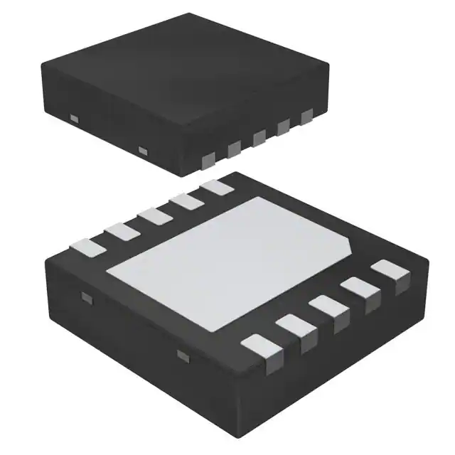
- Part No.:
- LM3658SD-A/NOPB
- Manufacturer:
- Texas Instruments
- Category:
- Battery Chargers
- Package:
- 10-WFDFN Exposed Pad
- Datasheet:
-
 LM3658SD-A/NOPB.pdf
- Description:
- IC BATT CHG LI-ION 1CELL 10WSON
- Quantity:
- Payment:

- Shipping:

Inventory:5,122
Please send an inquiry. Send us your inquiry, and we will respond immediately.
Product details
Overview
LM3658SD-A/NOPB from Texas Instruments is a dual-source Li-ion/polymer battery charger IC with integrated power FETs, automatic USB/AC wall adapter source selection, and 5–10 hour selectable charge timers. It delivers up to 1000 mA from AC or 500 mA from USB, maintains ±0.35% termination accuracy at 4.2 V, and operates in pre-qualification, constant-current, constant-voltage, top-off, and maintenance modes for portable devices.
For engineers reviewing the LM3658SD-A/NOPB datasheet, LM3658SD-A/NOPB pinout, LM3658SD-A/NOPB application, or LM3658SD-A/NOPB equivalent, key selection considerations include USB_sel–controlled timer selection (5 h vs. 10 h), ISET-resistor programmable AC charge current, thermal regulation at 120°C, open-drain STAT1/STAT2 status outputs, and TS-pin–based battery temperature monitoring using NTC thermistors.
Technical Context
The LM3658SD-A/NOPB implements a fully integrated linear charging architecture with dual-input power path management: CHG_IN (4.5–6.0 V) and USBpwr (4.35–6.0 V), where CHG_IN takes priority when both are present. Its internal thermal regulation dynamically limits charge current to maintain junction temperature at 120°C, independent of ambient conditions.
It supports two distinct operational configurations via USB_sel: pin-high enables 5-hour TCHG and 30-minute TTOPOFF for fast cycling; pin-low extends TCHG to 10 hours and TTOPOFF to 60 minutes-applicable in both CHG_IN and USBpwr modes. Unlike the LM3658SD-B, it does not support LDO mode; floating TS pin triggers suspend mode, not regulator operation.
Key Specifications
| Parameter | Value and Actual Design Meaning |
|---|---|
| Charge Termination Voltage | 4.2 V ±0.35% at 25°C - ensures precise full-charge cutoff critical for Li-ion cell longevity and safety |
| AC Full-Rate Charge Current | 50–1000 mA - set by external ISET resistor (e.g., 5 kΩ → ~500 mA), enabling flexible battery capacity matching |
| USB Charge Current Options | 100 mA or 500 mA - selected by USB_sel logic level, compliant with USB 2.0 port current limits |
| Charge Timer (TCHG) | Selectable 5 h (USB_sel = high) or 10 h (USB_sel = low) - prevents overcharge while accommodating diverse battery chemistries and capacities |
| Junction Temperature Regulation | Fixed at 120°C - thermally throttles charge current to prevent die overheating without external thermal sensors |
| Battery Temp Sensing | TS pin accepts NTC thermistor (10 kΩ @ 25°C) - monitors voltage window (0.49 V / 2.49 V thresholds) to suspend charging outside safe temp range |
| Quiescent Current (Power Down) | 1 µA typical - minimizes battery drain during idle, essential for always-on portable systems |
Pinout & Package
LM3658SD-A/NOPB uses a thermally enhanced 3 mm × 3 mm WSON-10 package with exposed die-attach pad (DAP) soldered to PCB ground for optimal thermal dissipation (θJA = 54°C/W with proper layout).
| Pin/Terminal | Circuit Role | Design Meaning |
|---|---|---|
| CHG_IN | AC wall adapter input | Accepts 4.5–6.0 V; primary power source with priority over USBpwr |
| USBpwr | USB power input | Accepts 4.35–6.0 V; secondary source activated only if CHG_IN is absent or invalid |
| GND | Power and signal reference | Common return for all circuits; must connect to DAP for thermal performance |
| USB_sel | USB current/timer select | Pull high → 500 mA USB charge + 5 h TCHG; pull low → 100 mA + 10 h TCHG |
| EN_b | Active-low enable | Pull low → enable charging; pull high → suspend with ultra-low 1 µA quiescent current |
| STAT2 | Open-drain status output | Active-low indicator: OFF = charge complete; ON+STAT1 = bad battery or suspend |
| STAT1 | Open-drain status output | Active-low indicator: ON = pre-qual, CC/CV, or top-off; OFF+STAT2 = done |
| ISET | Charge current programming | Resistor-to-GND sets AC charge current (ICHG = 2500 AΩ / RISET) |
| TS | Battery temperature sense | Connects to NTC thermistor; floating → suspend mode (not LDO); no battery detection |
| BATT | Battery positive terminal | Direct connection to single-cell Li-ion/polymer anode; Kelvin-sensed for accurate voltage regulation |
Key Features
| Feature | Design Value |
|---|---|
| Automatic dual-input source selection | CHG_IN always prioritized over USBpwr; seamless handover without host intervention |
| Programmable AC charge current | 50–1000 mA via single ISET resistor - eliminates need for external current-sense amplifiers |
| Selectable charge timers | USB_sel pin configures TCHG (5 h / 10 h) and TTOPOFF (30 min / 60 min) - supports wide battery capacity range |
| On-board Kelvin sensing | Separate BATT and ISET paths eliminate PCB trace IR drop error - achieves ±0.35% termination accuracy |
| Integrated safety timers | TPREQUAL (30 min), TCHG (5/10 h), TTOPOFF (30/60 min) - enforce hard limits on all charge phases |
| Continuous temperature monitoring | TS pin interface with internal 0.49 V / 2.49 V comparators - suspends charging outside 0°C–45°C (NTC-based) |
Applications
| Smartphones | Digital Still Cameras |
|---|---|
Use Scenario: Compact handheld device requiring dual-input charging (USB for desktop sync, AC for rapid top-up) with minimal external components. IC Role / Device Role / Timing Role: Primary Li-ion charger managing pre-qual, CC/CV, top-off, and maintenance cycles; STAT1/STAT2 drive status LEDs. Use Value: Eliminates discrete MOSFETs and sense resistors; 3 mm × 3 mm WSON footprint saves board space in tight camera modules. |
Use Scenario: Portable imaging device with intermittent USB connectivity and frequent AC charging, needing reliable full-charge completion. IC Role / Device Role / Timing Role: Battery management unit enforcing strict 4.2 V ±0.35% termination and 5-hour max charge time to preserve high-cycle-life cells. Use Value: Prevents overcharge-induced swelling in sealed camera enclosures; thermal regulation avoids heat buildup near image sensors. |
| PDAs | USB-powered MP3 Players |
Use Scenario: Legacy PDA with removable battery and dual-power capability, requiring graceful fallback between USB and AC sources. IC Role / Device Role / Timing Role: Dual-path power manager that auto-selects CHG_IN when available, else defaults to USBpwr with 100 mA limit unless USB_sel is high. Use Value: Enables "plug-and-play" charging without firmware configuration; suspend mode on TS disconnect prevents false battery-detection faults. |
Use Scenario: Flash-based audio player drawing power solely from USB bus during sync/charge, demanding strict compliance with USB current specs. IC Role / Device Role / Timing Role: USB-native charger enforcing 100 mA (USB_sel = low) or 500 mA (USB_sel = high) with built-in deglitch timing (TDGL = 20–80 ms). Use Value: Guarantees USB enumeration stability; prevents host port shutdown due to overcurrent - critical for mass-storage-class devices. |
Equivalent & Alternatives
The following parts are listed as comparable options for similar Li-ion charger IC applications.
| Alternative Part | Technical Difference | Application Difference | Selection Advice |
|---|---|---|---|
| BQ24075RGTR | Single-input (USB-only), fixed 4.2 V termination, no AC wall adapter support, 1.5 A max charge current | Lacks dual-source capability and programmable AC current; suited only for USB-centric designs | Select when design uses USB exclusively and requires higher current than LM3658SD-A/NOPB's 500 mA USB limit |
| TPS65023RSBR | Multi-rail PMIC with integrated 1.5 A charger, DC/DC converters, LDOs; supports AC/USB but requires external FETs for >1 A | Higher integration but larger 5 mm × 5 mm QFN package and greater complexity; not pin-compatible | Choose when system needs power sequencing, multiple regulated rails, and charger in one IC - at cost of board area and design effort |
Compared with BQ24075RGTR and TPS65023RSBR, the LM3658SD-A/NOPB uniquely balances dual-input autonomy, compact WSON-10 packaging, and USB_sel–driven timer flexibility - making it optimal for space-constrained, battery-first portable devices where AC fallback and precise charge control are mandatory.
Availability
LM3658SD-A/NOPB is available at Aetrix Electronics and suitable for smartphones, digital still cameras, PDAs, and USB-powered MP3 players requiring stable component supply, long-term lifecycle support, and consistent parametric performance across production batches.
Supply support for LM3658SD-A/NOPB includes scheduled delivery planning, volume procurement assistance, BOM continuity management, traceable sourcing, and lifecycle availability coordination for OEM customers, industrial embedded developers, connected-device designers, and electronics production programs.
Manufacturer
Texas Instruments is a global semiconductor leader specializing in analog, embedded processing, and power management technologies, with decades of expertise in battery charging solutions.
The LM3658 product line targets portable consumer electronics requiring highly integrated, thermally robust, and dual-source–capable Li-ion charging - designed to reduce bill-of-materials count and simplify layout for handheld form factors.
FAQ
What is the function of the USB_sel pin on the LM3658SD-A/NOPB?
The USB_sel pin on the LM3658SD-A/NOPB serves a dual function: it selects USB charge current (100 mA when pulled low, 500 mA when pulled high) and determines charge timer duration (10-hour TCHG and 60-minute TTOPOFF when low; 5-hour TCHG and 30-minute TTOPOFF when high). This behavior applies in both CHG_IN and USBpwr modes, and is a defining feature of the LM3658SD-A/NOPB variant.
Does the LM3658SD-A/NOPB support LDO mode when the TS pin is left floating?
No, the LM3658SD-A/NOPB does not support LDO mode. When the TS pin is left floating, the LM3658SD-A/NOPB enters suspend mode - halting charging and asserting both STAT1 and STAT2 high - unlike the LM3658SD-B version, which invokes LDO mode under the same condition. This distinction is explicitly documented in the TI datasheet SNVS328E.
How is the full-rate AC charge current programmed on the LM3658SD-A/NOPB?
The full-rate AC charge current on the LM3658SD-A/NOPB is programmed using an external resistor (RISET) connected between the ISET pin and GND, per the equation ICHG = 2500 AΩ / RISET. For example, a 5 kΩ resistor yields ~500 mA. This setting is independent of USB_sel and applies only during CHG_IN operation; USB charge current is controlled solely by USB_sel logic level.
What thermal performance can be expected from the LM3658SD-A/NOPB WSON-10 package?
The LM3658SD-A/NOPB WSON-10 package achieves θJA = 54°C/W when the exposed die-attach pad (DAP) is soldered to a grounded thermal land with ≥4 thermal vias (0.33 mm diameter, 1.27 mm pitch). Without this layout, thermal resistance degrades significantly. Internal thermal regulation holds junction temperature at 120°C, dynamically reducing charge current to prevent exceeding this limit.
What happens if the battery voltage drops below 3.94 V after full charge completion on the LM3658SD-A/NOPB?
If the battery voltage drops below 3.94 V (VRESTART threshold) after maintenance mode begins, the LM3658SD-A/NOPB automatically initiates a new full-rate charge cycle - reactivating STAT1 (ON), turning off STAT2, and resetting all timers. This recharge behavior ensures battery voltage remains within operational range without host processor intervention, supporting true "set-and-forget" portable operation.
LM3658SD-A/NOPB Specifications
- Product attributes
- Attribute value
- Manufacturer:
- Texas Instruments
- Series:
- -
- Package/Case:
- 10-WFDFN Exposed Pad
- Packaging:
- Tape & Reel (TR)
- Product Status:
- Active
- Battery Chemistry:
- Lithium Ion/Polymer
- Number of Cells:
- 1
- Current - Charging:
- Constant - Programmable
- Programmable Features:
- -
- Fault Protection:
- Over Current, Over Temperature
- Charge Current - Max:
- 1A
- Battery Pack Voltage:
- 4.2V
- Voltage - Supply (Max):
- 6V
- Interface:
- USB
- Operating Temperature:
- -40°C ~ 85°C (TA)
- Grade:
- -
- Qualification:
- -
- Mounting Type:
- Surface Mount
- Supplier Device Package:
- 10-WSON (3x3)
LM3658SD-A/NOPB FAQ
1.How can I place an order for LM3658SD-A/NOPB through Aetrix?
Please submit a Request for Quotation (RFQ) for LM3658SD-A/NOPB on Aetrix. Our sales agent will provide a competitive quotation and guide you through the order confirmation once you accept the terms.
2.Are the price and stock information for LM3658SD-A/NOPB reliable?
The price and inventory of LM3658SD-A/NOPB are updated periodically and may fluctuate due to market conditions. Stock and pricing data are typically refreshed every 24 hours. Quotation validity for LM3658SD-A/NOPB is usually 5 days.
3.What payment methods are accepted for LM3658SD-A/NOPB?
We accept Wire Transfer, PayPal, Credit Card, Western Union, MoneyGram, and Escrow for LM3658SD-A/NOPB transactions.
Note: Certain payment methods may incur a processing fee.
4.How is shipping managed for LM3658SD-A/NOPB?
LM3658SD-A/NOPB orders can be shipped via leading logistics carriers, including DHL, UPS, FedEx, TNT, or Registered Mail.
Once your LM3658SD-A/NOPB order is processed, you will receive an email with the shipment details and tracking number.
Note: Tracking information may take up to 24 hours to appear. Express delivery typically takes 3–5 business days.
5.How can I obtain technical support or documentation for LM3658SD-A/NOPB?
For technical support, including LM3658SD-A/NOPB datasheets, pinout diagrams, or application guidance, please contact our engineering support team. They can provide detailed documentation and assistance for your LM3658SD-A/NOPB requirements.
6.How does Aetrix verify that LM3658SD-A/NOPB is sourced from the original manufacturer or authorized distributors?
All LM3658SD-A/NOPB products on Aetrix are procured from qualified distributors and authorized channels. Our dedicated quality assurance team conducts strict verification, including traceability checks and, if necessary, third-party testing. This ensures that LM3658SD-A/NOPB meets industry standards.
7.What is the process for return or replacement of LM3658SD-A/NOPB?
All LM3658SD-A/NOPB units undergo pre-shipment inspection (PSI). If there is an issue with LM3658SD-A/NOPB, returns or replacements are accepted under the following conditions:
1.Quantity discrepancies, incorrect items, or visible external defects (such as breakage or corrosion), acknowledged by Aetrix.
2.The issue is reported within 90 days of delivery.
3.The LM3658SD-A/NOPB part is unused and in its original packaging.
Return procedure for LM3658SD-A/NOPB:
1.Submit a request within 90 days.
2.Obtain a Return Material Authorization (RMA) from Aetrix.
LM3658SD-A/NOPB Tags

-
BQ21040DBVR
Texas Instruments

-
MCP73812T-420I/OT
Microchip Technology
-
MCP73831T-2ACI/OT
Microchip Technology
-
MCP73832T-2ACI/OT
Microchip Technology
-
MCP73831T-2DCI/OT
Microchip Technology
-
MCP73832T-2DCI/OT
Microchip Technology
-
MCP73831T-2ATI/OT
Microchip Technology
-
MCP73832T-2ATI/OT
Microchip Technology
-
MCP73831T-5ACI/OT
Microchip Technology

-
MCP73832T-2ACI/MC
Microchip Technology
-
MCP73831T-2ACI/MC
Microchip Technology
-
MCP73831T-2ATI/MC
Microchip Technology
Tech Hub

A practical engineering guide to 3.3V and 5V logic compatibility, input thresholds, resistor dividers, translator ICs, MOSFET level shifting, I2C pull-ups, timing limits and power-sequencing risks.

The 74HC595 uses push-pull logic outputs, while the TPIC6B595 uses 50 V open-drain DMOS sinks for higher-power loads. This guide compares timing, current limits, 3.3 V interfacing, load wiring, thermal…

The 74HC595 converts serial data into eight stable parallel outputs. This guide covers pin functions, shift and storage timing, OE and MR behavior, drive-current limits, cascading, voltage compatibilit…

A technical comparison of level-sensitive latches and edge-triggered flip-flops, covering timing windows, setup and hold limits, master–slave operation, time borrowing, race-through, HDL inference and…

A D latch stores one bit while Enable controls when data can pass. This reference covers gate-level operation, truth tables, transparency, setup and hold timing, LE versus OE, common ICs and practical …

An SR latch stores one bit through cross-coupled feedback. This engineering reference covers NOR and NAND implementations, truth tables, forbidden-state recovery, gated operation, switch debouncing, fa…

Latch circuits retain one bit through feedback. This technical reference covers SR and D latches, truth tables, transparency, timing limits, latch-versus-flip-flop behavior, applications and common log…

An engineering guide to LED driver operation, constant-current and constant-voltage outputs, linear and switching topologies, dimming, IC selection, calculations, replacement compatibility, and fault c…

Operational amplifier guide covering op amp basics, feedback, ideal vs real op amps, common configurations, buffer circuits, offset, bias current, gain-bandwidth, slew rate, rail-to-rail limits and sel…

Jumper cables guide covering safe connection order, red and black clamp placement, final ground connection, cable gauge, length, clamp quality, copper vs CCA cables, jump starter comparison and battery…


