
 My Inquiry
 My Account


Texas Instruments LM8323JGR8AXMX/NOPB
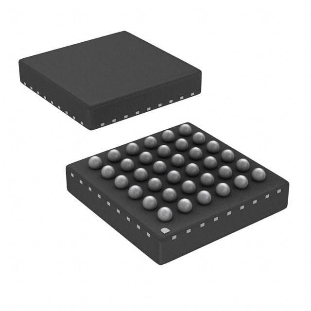
- Part No.:
- LM8323JGR8AXMX/NOPB
- Manufacturer:
- Texas Instruments
- Category:
- Controllers
- Package:
- 36-TFBGA
- Datasheet:
-
 LM8323JGR8AXMX/NOPB.pdf
- Description:
- IC CONTROLLER I2C 36CSBGA
- Quantity:
- Payment:

- Shipping:

Inventory:4,356
Please send an inquiry. Send us your inquiry, and we will respond immediately.
Product details
Overview
LM8323JGR8AXMX/NOPB from Texas Instruments is a dedicated mobile I/O companion IC for keypad scanning, I/O expansion, and PWM-controlled LED brightness modulation. It operates from a 1.8V ±180 mV supply, supports up to 8×12 keypad matrices plus 8 special-function keys (104 total), and communicates via I²C-compatible ACCESS.bus at up to 400 kHz in slave mode - deployed in smart handheld devices requiring low-power, interrupt-driven key event handling.
For engineers reviewing the LM8323JGR8AXMX/NOPB datasheet, LM8323JGR8AXMX/NOPB pinout, LM8323JGR8AXMX/NOPB application, or LM8323JGR8AXMX/NOPB equivalent, this page delivers verified pin functions, real-world timing behavior (4 ms scan cycle, 12 ms default debounce), FIFO-based key-event buffering (15-event depth), and confirmed Halt-mode current (<9 µA at 1.98 V, 25°C).
Technical Context
The LM8323JGR8AXMX/NOPB integrates a hardware key-scan engine with configurable matrix size (up to 8×12), dedicated SF-key inputs that pull KP-X lines directly to ground, and three programmable PWM outputs clocked by either internal 2 MHz ÷64 (~32 kHz) or external 32.768 kHz sources. Its interrupt-driven architecture uses an open-drain IRQ output to signal key events, errors, or rotary encoder changes.
It features on-chip power-on reset (POR), watchdog timer, and a fully static design enabling true Halt mode with sub-9 µA standby current. Keypad events are stored in a 15-deep FIFO buffer with MSB-encoded press/release flags, and initialization requires host-configured parameters including SET_KEY_SIZE, SET_DEBOUNCE (1–255 cycles), and WRITE_CLOCK for clock source selection.
Key Specifications
| Parameter | Value and Actual Design Meaning |
|---|---|
| Supply Voltage | 1.8 V ±180 mV - enables direct interface with 1.8 V logic domains without level-shifting. |
| Keypad Support | Up to 8×12 matrix + 8 SF keys - provides 104 distinct key positions with priority override for SF keys. |
| I²C/ACCESS.bus Speed | Up to 400 kHz Fast-mode - ensures responsive host communication in compact handheld systems. |
| PWM Outputs | Three independent channels - support smooth LED dimming with ramp-up/ramp-down control. |
| FIFO Depth | 15-event buffer - prevents key loss during host latency; stores press/release codes with MSB flagging. |
| Halt Mode Current | <9 µA at 1.98 V, 25°C - enables ultra-low-power operation between user interactions. |
| Operating Temperature | −40°C to +85°C - qualified for industrial and portable consumer environments. |
| Scan Cycle Time | ~4 ms - defines minimum inter-event resolution and sets baseline for debounce timing. |
Pinout & Package
LM8323JGR8AXMX/NOPB uses a 36-pin csBGA package (package code NYB0036A), measuring 3.5 mm × 3.5 mm with 0.5 mm pitch. Pin functions are validated per TI SNLS273A datasheet Rev. March 2013.
| Pin/Terminal | Circuit Role | Design Meaning |
|---|---|---|
| KP-X0–KP-X7 | Keypad row inputs / wake-up inputs | High-impedance after reset; configured as keypad scan inputs with on-chip pullups - SF keys connect these directly to ground. |
| KP-Y0–KP-Y11 | Keypad column outputs | Driven low during active scan; support up to 12 columns; KP-Y9–KP-Y11 shared with rotary encoder when enabled. |
| ACB_SDA / ACB_SCL | ACCESS.bus interface | I²C-compatible bidirectional data/clock; open-drain with internal weak pullups - requires external pullups for reliable bus operation. |
| PWM_0–PWM_2 | Pulse-width modulated outputs | Three independent PWM drivers; PWM_2 shares pin with GPIO_15 and CONFIG_2 - function selected at runtime. |
| IRQ | Interrupt request output | Open-drain active-low signal; asserts on key events, errors, or rotary encoder changes - programmable push-pull mode available. |
| CONFIG_1 / CONFIG_2 | Slave address select inputs | Determine 7-bit ACCESS.bus address (1000010X–1000101X); double as GPIO after reset initialization. |
| XTAL_IN / XTAL_OUT | 32.768 kHz crystal interface | Support external crystal for precise PWM timing; XTAL_IN is alternate function of SLOWCLK input. |
| SLOWCLKOUT | 32.768 kHz buffered clock output | Alternate function of KP-Y8/GPIO_03; enables clock distribution to other system components when enabled. |
Key Features
| Feature | Design Value |
|---|---|
| Hardware key-scan engine | Offloads host CPU from polling; handles matrix decoding, debouncing, and FIFO storage autonomously. |
| Special-function (SF) key support | Eight dedicated ground-switched inputs that override standard keypad rows - enables wake-from-halt via physical keypress. |
| Configurable Halt mode | Enters ultra-low-power state after programmable inactivity period (4–1020 ms); exits on keypress, bus activity, or rotary change. |
| Rotary encoder interface | Shares KP-Y9/Y10/Y11 pins; supports incremental encoder counting - disabled by default, enabled via host command. |
| GPIO expansion capability | 16 general-purpose I/Os (GPIO_00–GPIO_15); configurable as input/output with programmable pullup/pulldown - usable on unused keypad pins. |
| On-chip power-on reset (POR) | Guarantees known initial state at power-up; threshold ~1.2–1.5 V; requires VCC rise time 20 µs–10 ms for reliable assertion. |
Applications
| Smartphone Keypad Interface | Feature-Rich Cordless Phone UI |
|---|---|
Use Scenario: Managing QWERTY-style alphanumeric keypad with backlight dimming and wake-on-keypress in battery-powered smartphones. IC Role / Device Role / Timing Role: Dedicated key-scan controller with integrated 15-event FIFO, PWM-driven LED backlight, and Halt-mode power management. Use Value: Reduces host processor load by >90% vs. software scanning; achieves <9 µA standby current; supports simultaneous multi-key detection across rows. |
Use Scenario: Supporting 8×9 keypad plus 8 SF keys (e.g., speakerphone, mute, redial) with dynamic LED status indicators in DECT cordless handsets. IC Role / Device Role / Timing Role: Centralized I/O companion handling key matrix, rotary volume control, and three independent PWM outputs for LED feedback. Use Value: Eliminates need for discrete GPIO expanders and LED drivers; enables wake-from-halt on any SF key; maintains 4 ms scan resolution for tactile response. |
| Industrial Handheld Terminal | Medical Patient Monitor Keypad |
Use Scenario: Ruggedized barcode scanner or asset tracker requiring reliable key entry under ESD stress and wide temperature range. IC Role / Device Role / Timing Role: Robust keypad interface with 12 ms hardware debounce, on-chip POR, and −40°C to +85°C operation. Use Value: Prevents false key registration from mechanical bounce or noise; survives repeated ESD events via integrated protection; no firmware tuning required. |
Use Scenario: Critical-care patient monitor with silent, responsive keypad for alarm silencing and parameter adjustment in low-noise clinical environments. IC Role / Device Role / Timing Role: Low-power, interrupt-driven key handler with error-detection (FIFOOVR/KEYOVR), IRQ signaling, and fail-safe reset behavior. Use Value: Guarantees keypress capture even during Halt-mode transitions (FW6 firmware); reports overflow errors before data loss; supports audit-trail logging via FIFO readout. |
Equivalent & Alternatives
The following parts are listed as comparable options for similar key-scan and I/O expansion applications.
| Alternative Part | Technical Difference | Application Difference | Selection Advice |
|---|---|---|---|
| TCA6424A | 24-bit I²C GPIO expander with interrupt but no native key-scan engine or PWM outputs. | Requires host-side key matrix scanning logic and external LED drivers. | Select when system already implements key-scan firmware and needs only GPIO extension. |
| MAX7347 | 8×8 keypad scanner with 8 GPIOs and 2 PWMs; supports 1.8 V operation but lacks SF-key priority and rotary encoder interface. | Maximum 64 keys (no SF-key override); no Halt-mode current spec below 10 µA. | Select for simpler 8×8 layouts where SF-key wake-up and ultra-low standby are not required. |
Compared with TCA6424A and MAX7347, LM8323JGR8AXMX/NOPB uniquely integrates hardware-accelerated key-scan, 104-key capacity with SF-key priority, three PWMs, and sub-9 µA Halt-mode current - making it optimal for space-constrained, battery-sensitive handhelds needing zero-host-scan overhead.
Availability
LM8323JGR8AXMX/NOPB is available at Aetrix Electronics and suitable for smart handheld devices, cordless telephony systems, and industrial handheld terminals requiring stable component supply, long-term lifecycle support, and guaranteed traceable sourcing.
Supply support for LM8323JGR8AXMX/NOPB includes scheduled delivery planning, volume procurement assistance, BOM continuity management, traceable sourcing, and lifecycle availability coordination for OEM customers, industrial embedded developers, connected-device designers, and electronics production programs.
Manufacturer
Texas Instruments is a global semiconductor leader specializing in analog, embedded processing, and connectivity technologies, with decades of expertise in low-power mixed-signal IC design.
The LM8323JGR8AXMX/NOPB belongs to TI's Mobile I/O Companion product line, engineered specifically to offload keypad scanning, I/O expansion, and LED dimming tasks from application processors in portable electronics.
FAQ
What is the maximum keypad matrix size supported by LM8323JGR8AXMX/NOPB?
The LM8323JGR8AXMX/NOPB supports up to an 8×12 keypad matrix plus eight special-function (SF) keys, totaling 104 distinct key positions. When the rotary encoder interface is enabled, KP-Y9 through KP-Y11 are reassigned, reducing maximum matrix size to 8×9 while retaining all eight SF keys. This configuration is confirmed in the SNLS273A datasheet section "Key Device Characteristics" and Figure 2.
Does LM8323JGR8AXMX/NOPB require an external crystal for PWM operation?
No - LM8323JGR8AXMX/NOPB can operate its PWM outputs using the internal 2 MHz clock divided by 64 (~32 kHz), which is the default setting after reset. An external 32.768 kHz crystal (across XTAL_IN/XTAL_OUT) or clock (on SLOWCLK) is optional and used only when higher PWM timing precision is required. The WRITE_CLOCK command selects the source, as defined in Table 1 of SNLS273A.
How does LM8323JGR8AXMX/NOPB handle multiple simultaneous key presses?
LM8323JGR8AXMX/NOPB stores all detected key-press and key-release events in its 15-event FIFO buffer in chronological order. It reliably captures multiple key presses located in different KP-X rows. However, ambiguity arises if ≥2 keys in the same row are pressed simultaneously - in that case, the device reports a KEYOVR error and asserts IRQ. Host firmware must read READ_ERROR and clear the FIFO to resume normal operation.
What is the function of the CONFIG_1 and CONFIG_2 pins on LM8323JGR8AXMX/NOPB after initialization?
After power-on reset and host initialization, CONFIG_1 and CONFIG_2 on LM8323JGR8AXMX/NOPB become general-purpose I/O ports (GPIO_14 and GPIO_15), as documented in Table 2 ("Pin Configuration After Reset") and the "INITIALIZATION" section of SNLS273A. They retain this dual role unless explicitly reconfigured by the host via WRITE_PORT_SEL and WRITE_PORT_STATE commands.
What is the minimum debounce time achievable with LM8323JGR8AXMX/NOPB?
The minimum debounce time for LM8323JGR8AXMX/NOPB is one scan cycle, or approximately 4 ms, set via the SET_DEBOUNCE command with parameter value 0x01. This value corresponds to the shortest delay between detecting a keypad state change and confirming it before asserting IRQ - verified in the "Timing Parameters" section and Table 5 of SNLS273A.
LM8323JGR8AXMX/NOPB Specifications
- Product attributes
- Attribute value
- Manufacturer:
- Texas Instruments
- Package/Case:
- 36-TFBGA
- Programmable:
- Not Verified
- Protocol:
- -
- Function:
- Controller
- Interface:
- I2C
- Standards:
- -
- Voltage - Supply:
- 1.62V ~ 1.98V
- Current - Supply:
- 1.9mA
- Operating Temperature:
- -40°C ~ 85°C
- Supplier Device Package:
- 36-CSBGA (3.5x3.5)
- Grade:
- -
- Qualification:
- -
LM8323JGR8AXMX/NOPB FAQ
1.How can I place an order for LM8323JGR8AXMX/NOPB through Aetrix?
Please submit a Request for Quotation (RFQ) for LM8323JGR8AXMX/NOPB on Aetrix. Our sales agent will provide a competitive quotation and guide you through the order confirmation once you accept the terms.
2.Are the price and stock information for LM8323JGR8AXMX/NOPB reliable?
The price and inventory of LM8323JGR8AXMX/NOPB are updated periodically and may fluctuate due to market conditions. Stock and pricing data are typically refreshed every 24 hours. Quotation validity for LM8323JGR8AXMX/NOPB is usually 5 days.
3.What payment methods are accepted for LM8323JGR8AXMX/NOPB?
We accept Wire Transfer, PayPal, Credit Card, Western Union, MoneyGram, and Escrow for LM8323JGR8AXMX/NOPB transactions.
Note: Certain payment methods may incur a processing fee.
4.How is shipping managed for LM8323JGR8AXMX/NOPB?
LM8323JGR8AXMX/NOPB orders can be shipped via leading logistics carriers, including DHL, UPS, FedEx, TNT, or Registered Mail.
Once your LM8323JGR8AXMX/NOPB order is processed, you will receive an email with the shipment details and tracking number.
Note: Tracking information may take up to 24 hours to appear. Express delivery typically takes 3–5 business days.
5.How can I obtain technical support or documentation for LM8323JGR8AXMX/NOPB?
For technical support, including LM8323JGR8AXMX/NOPB datasheets, pinout diagrams, or application guidance, please contact our engineering support team. They can provide detailed documentation and assistance for your LM8323JGR8AXMX/NOPB requirements.
6.How does Aetrix verify that LM8323JGR8AXMX/NOPB is sourced from the original manufacturer or authorized distributors?
All LM8323JGR8AXMX/NOPB products on Aetrix are procured from qualified distributors and authorized channels. Our dedicated quality assurance team conducts strict verification, including traceability checks and, if necessary, third-party testing. This ensures that LM8323JGR8AXMX/NOPB meets industry standards.
7.What is the process for return or replacement of LM8323JGR8AXMX/NOPB?
All LM8323JGR8AXMX/NOPB units undergo pre-shipment inspection (PSI). If there is an issue with LM8323JGR8AXMX/NOPB, returns or replacements are accepted under the following conditions:
1.Quantity discrepancies, incorrect items, or visible external defects (such as breakage or corrosion), acknowledged by Aetrix.
2.The issue is reported within 90 days of delivery.
3.The LM8323JGR8AXMX/NOPB part is unused and in its original packaging.
Return procedure for LM8323JGR8AXMX/NOPB:
1.Submit a request within 90 days.
2.Obtain a Return Material Authorization (RMA) from Aetrix.
LM8323JGR8AXMX/NOPB Tags

-
PTN5150AHXMP
NXP Semiconductors

-
USB3740B-AI9-TR
Microchip Technology

-
USB3740B-AI2-TR
Microchip Technology

-
USB3300-EZK-TR
Microchip Technology
-
USB3300-EZK
Microchip Technology

-
FUSB340TMX
onsemi

-
FUSB302BMPX
onsemi

-
DP83826IRHBR
Texas Instruments

-
MCP2518FDT-E/QBB
Microchip Technology
-
FUSB302MPX
onsemi

-
MCP2518FDT-E/SL
Microchip Technology

-
FT260Q-R
FTDI, Future Technology Devices International Ltd
Tech Hub

A practical engineering guide to 3.3V and 5V logic compatibility, input thresholds, resistor dividers, translator ICs, MOSFET level shifting, I2C pull-ups, timing limits and power-sequencing risks.

The 74HC595 uses push-pull logic outputs, while the TPIC6B595 uses 50 V open-drain DMOS sinks for higher-power loads. This guide compares timing, current limits, 3.3 V interfacing, load wiring, thermal…

The 74HC595 converts serial data into eight stable parallel outputs. This guide covers pin functions, shift and storage timing, OE and MR behavior, drive-current limits, cascading, voltage compatibilit…

A technical comparison of level-sensitive latches and edge-triggered flip-flops, covering timing windows, setup and hold limits, master–slave operation, time borrowing, race-through, HDL inference and…

A D latch stores one bit while Enable controls when data can pass. This reference covers gate-level operation, truth tables, transparency, setup and hold timing, LE versus OE, common ICs and practical …

An SR latch stores one bit through cross-coupled feedback. This engineering reference covers NOR and NAND implementations, truth tables, forbidden-state recovery, gated operation, switch debouncing, fa…

Latch circuits retain one bit through feedback. This technical reference covers SR and D latches, truth tables, transparency, timing limits, latch-versus-flip-flop behavior, applications and common log…

An engineering guide to LED driver operation, constant-current and constant-voltage outputs, linear and switching topologies, dimming, IC selection, calculations, replacement compatibility, and fault c…

Operational amplifier guide covering op amp basics, feedback, ideal vs real op amps, common configurations, buffer circuits, offset, bias current, gain-bandwidth, slew rate, rail-to-rail limits and sel…

Jumper cables guide covering safe connection order, red and black clamp placement, final ground connection, cable gauge, length, clamp quality, copper vs CCA cables, jump starter comparison and battery…


