
 My Inquiry
 My Account


Texas Instruments LM8327JGR8/NOPB
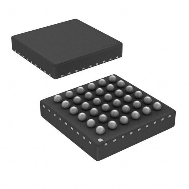
- Part No.:
- LM8327JGR8/NOPB
- Manufacturer:
- Texas Instruments
- Category:
- Specialized
- Package:
- 36-TFBGA
- Datasheet:
-
 LM8327JGR8/NOPB.pdf
- Description:
- IC INTFACE SPECIALIZED 36CSBGA
- Quantity:
- Payment:

- Shipping:

Inventory:1,752
Please send an inquiry. Send us your inquiry, and we will respond immediately.
Product details
Overview
LM8327JGR8/NOPB from Texas Instruments is a mobile I/O companion IC designed to offload keypad scanning and LED PWM control from host processors in handheld devices. It integrates an 8×12 keypad controller with 8 SF keys (104-key total), three independent programmable PWM outputs for smooth LED brightness modulation, and an I²C-compatible ACCESS.bus slave interface operating at 100 kHz/400 kHz. Its 1.8V ±10% single-supply operation and −40°C to +85°C temperature range support cordless phones and smart handheld applications.
For engineers reviewing the LM8327JGR8/NOPB datasheet, LM8327JGR8/NOPB pinout, LM8327JGR8/NOPB application, or LM8327JGR8/NOPB equivalent, key selection considerations include its dedicated keypad event buffer (15-byte FIFO), automatic HALT mode entry after 1020 ms inactivity, on-chip RC oscillator eliminating external clock requirements, ESD glitch filtering on RESETN, and support for up to 26 direct-connect keys with wake-up capability.
Technical Context
The LM8327JGR8/NOPB implements a register-based command interpreter with auto-increment addressing for efficient multi-byte I²C access. Its keyscan engine performs full matrix evaluation every 4 ms, storing press/release events in a FIFO and supporting up to four simultaneous key presses via KBDCODE[3:0] registers.
Each of its three PWM channels operates from a dedicated 32.768 kHz slow clock, executing self-sustaining scripts (up to 32 commands per 64-byte buffer) including RAMP, SET_PWM, GO_TO_START, BRANCH, and TRIGGER instructions - enabling synchronized LED fading without host intervention.
Key Specifications
| Parameter | Value and Actual Design Meaning |
|---|---|
| Interface | I²C-compatible ACCESS.bus slave only, 100 kHz standard-mode / 400 kHz fast-mode |
| Keypad Support | Up to 8×12 matrix (96 keys) + 8 special function keys = 104-key total; also supports 26 direct-connect keys |
| PWM Outputs | Three independent channels, each with 64-byte script buffer supporting RAMP, SET_PWM, BRANCH, and TRIGGER commands |
| Supply Voltage | 1.8 V ±10%, enabling direct integration into low-voltage mobile power domains |
| Operating Temp | −40°C to +85°C, qualified for industrial-grade handheld and cordless phone environments |
| Package | 36-pin csBGA (NYB0036A), 3.5 mm × 3.5 mm × 0.8 mm, suitable for space-constrained PCB layouts |
| Power Management | Automatic HALT mode reduces current consumption; wake-up triggered by IRQ edge, pulse, or ACCESS.bus activity |
Pinout & Package
LM8327JGR8/NOPB uses a 36-pin chip-scale ball grid array (csBGA) package designated NYB0036A, measuring 3.5 mm × 3.5 mm × 0.8 mm with 0.5 mm ball pitch. All pins support multiple functions (keypad I/O, GPIO, PWM, or interrupt), configured via register settings at startup.
| Pin/Terminal | Circuit Role | Design Meaning |
|---|---|---|
| IRQN | Open-drain interrupt output | Asserts low on key event, error, or hardware interrupt; includes ESD glitch filter and polarity-selectable edge detection |
| SCL / SDA | I²C-compatible ACCESS.bus interface | Supports 100 kHz / 400 kHz communication; requires external pull-ups; handles clock stretching during busy periods |
| RESETN | Active-low reset input | Includes internal ESD glitch filter; drives low after POR until RSTINTCLR register (0x84) is written with 0x01 |
| PWM0–PWM2 | Dedicated PWM output terminals | Each driven by independent slow-clock (32.768 kHz) timer with script-execution capability; no host polling required |
| KPX0–KPX7 / KPY0–KPY11 | Keypad matrix row/column I/O | Configurable as inputs with on-chip pull-ups/downs; support full 8×12 scan or partial matrix configurations |
| DIRECT0–DIRECT25 | Direct key input terminals | 26 pins configurable as Schmitt-trigger inputs with programmable debounce (e.g., 12 ms); support wake-up from HALT mode |
Key Features
| Feature | Design Value |
|---|---|
| On-chip RC oscillator | Eliminates need for external crystal or clock source - reduces BOM count and board area |
| 15-byte key event FIFO | Stores sequential press/release events with timestamp-like ordering; prevents loss during host latency |
| Programmable autosleep timeout | Default 1020 ms inactivity triggers HALT mode; configurable via autosleep register to balance responsiveness and power |
| Dedicated slow clock input | Accepts 32 kHz to 8 MHz external clock on CLKIN for precise PWM timing or alternative system synchronization |
| Register-based command interpreter | Enables host configuration of keypad size, debounce time, pull resistors, interrupt masking, and PWM scripts via I²C |
Applications
| Cordless Phone Keypad Interface | Smart Handheld Device LED Control |
|---|---|
|
Use Scenario: Managing 4×8 mechanical keypad plus 8 SF keys in DECT cordless handsets with minimal host CPU overhead. IC Role / Device Role / Timing Role: Dedicated keypad controller with 4-ms scan interval, 15-byte FIFO buffering, and IRQ-driven event reporting. Use Value: Reduces host polling burden and ensures reliable key detection even during burst data transmission or RF activity. |
Use Scenario: Driving RGB backlight or status LEDs in battery-powered PDAs or barcode scanners requiring smooth brightness transitions. IC Role / Device Role / Timing Role: Autonomous PWM generator using 32.768 kHz clock and on-chip script execution for fade-in/fade-out effects. Use Value: Enables visually consistent LED behavior without consuming host processor cycles or requiring real-time OS scheduling. |
| Keyboard Expansion for Embedded Hosts | Low-Power Remote Control Interface |
|
Use Scenario: Adding 26 direct-connect tactile keys to microcontroller-based remote controls where GPIOs are constrained. IC Role / Device Role / Timing Role: General-purpose I/O expander with wake-up-capable inputs and programmable debounce (e.g., 12 ms). Use Value: Eliminates need for external debounce circuitry and allows host to remain in deep sleep until key press occurs. |
Use Scenario: Supporting both matrix keypad and direct keys in IR remotes with strict standby current limits (<1 µA typical in HALT mode). IC Role / Device Role / Timing Role: Power-aware I/O companion with automatic HALT entry and wake-up on any key or bus activity. Use Value: Achieves ultra-low quiescent current while maintaining responsive user interface - critical for coin-cell operation. |
Equivalent & Alternatives
The following parts are listed as comparable options for similar I/O companion and keypad controller applications.
| Alternative Part | Technical Difference | Application Difference | Selection Advice |
|---|---|---|---|
| TCA6424A | 24-bit I²C GPIO expander with interrupt but no integrated keypad scan engine or PWM | Lacks native keyscan logic, event FIFO, and autonomous PWM scripting - requires host firmware for key detection | Choose when only general-purpose I/O expansion is needed and host can manage scanning logic |
| MAX7359 | Keypad controller with 8×8 matrix support and 4 PWM outputs; operates at 2.7–5.5 V, not 1.8 V | Higher voltage requirement incompatible with 1.8 V mobile SoCs; larger 40-pin TQFN package | Consider only if system supply exceeds 2.5 V and board space permits larger footprint |
Compared with TCA6424A and MAX7359, LM8327JGR8/NOPB uniquely combines 104-key matrix support, 26 direct-key inputs, three scriptable PWM channels, and 1.8 V operation in a 3.5 mm × 3.5 mm csBGA - making it the only option that fully replaces host-side keyscan and LED control firmware in space- and power-constrained handheld designs.
Availability
LM8327JGR8/NOPB is available at Aetrix Electronics and suitable for cordless phones, smart handheld devices, keyboard applications, and remote controls requiring stable component supply across extended production lifecycles.
Supply support for LM8327JGR8/NOPB includes scheduled delivery planning, volume procurement assistance, BOM continuity management, traceable sourcing, and lifecycle availability coordination for OEM customers, industrial embedded developers, connected-device designers, and electronics production programs.
Manufacturer
Texas Instruments is a global semiconductor company headquartered in Dallas, Texas, delivering analog and embedded processing solutions for industrial, automotive, and personal electronics markets.
LM8327JGR8/NOPB belongs to TI's Mobile I/O Companion product line, engineered specifically to reduce host processor load in portable devices by integrating keyscan, I/O expansion, and autonomous LED PWM control in a single low-voltage IC.
FAQ
What is the default I²C address of the LM8327JGR8/NOPB after power-on reset?
The LM8327JGR8/NOPB defaults to I²C slave address 0x8A after power-on reset or Global Call Reset. This address can be reprogrammed via the ACCESS.bus interface, but the device will revert to 0x8A upon receiving a Global Call Reset command (write 0x06 to slave address 0x00). The LM8327JGR8/NOPB does not support hardware address pins, so all units share the same default unless modified in firmware.
Does the LM8327JGR8/NOPB require an external crystal or clock source?
No, the LM8327JGR8/NOPB includes an internal RC oscillator sufficient for keyscan and ACCESS.bus timing, eliminating the need for an external crystal. However, it does provide a CLKIN pin accepting 32 kHz to 8 MHz inputs for applications requiring higher PWM timing accuracy or system-level clock synchronization - the LM8327JGR8/NOPB operates correctly with or without this external signal.
How many simultaneous key presses can the LM8327JGR8/NOPB detect and report?
The LM8327JGR8/NOPB supports detection and storage of up to four simultaneous key presses. These are captured in KBDCODE0–KBDCODE3 registers, with the MULTIKEY flag indicating multi-key conditions. All events are also logged in the 15-byte EVTCODE FIFO, preserving chronological order for host retrieval - ensuring no key event is lost even during rapid multi-key interaction on the LM8327JGR8/NOPB.
Can the LM8327JGR8/NOPB wake up from HALT mode using only keypad activity?
Yes, the LM8327JGR8/NOPB wakes from HALT mode on any keypad activity - including key press, key release, or direct key transition - provided the corresponding interrupt sources are enabled in KBDMSK and DKBDMSK registers. Wake-up is edge- or pulse-triggered and asserts IRQN to notify the host, allowing the LM8327JGR8/NOPB to resume full operation within microseconds of user input.
What is the purpose of the 64-byte script buffer in each PWM channel of the LM8327JGR8/NOPB?
The 64-byte script buffer per PWM channel stores up to 32 executable instructions (e.g., RAMP, SET_PWM, BRANCH) that define autonomous LED behavior - such as fade sequences or color cycling - without host involvement. Once loaded and started, the LM8327JGR8/NOPB executes these scripts using its internal 32.768 kHz clock, freeing the host CPU and enabling precise, repeatable lighting effects independent of system load or software latency.
LM8327JGR8/NOPB Specifications
- Product attributes
- Attribute value
- Manufacturer:
- Texas Instruments
- Series:
- -
- Package/Case:
- 36-TFBGA
- Packaging:
- Tape & Reel (TR)
- Product Status:
- Active
- Applications:
- Mobile Communications
- Interface:
- I2C
- Voltage - Supply:
- 1.62V ~ 1.98V
- Supplier Device Package:
- 36-CSBGA (3.5x3.5)
- Grade:
- -
- Qualification:
- -
- Mounting Type:
- Surface Mount
LM8327JGR8/NOPB FAQ
1.How can I place an order for LM8327JGR8/NOPB through Aetrix?
Please submit a Request for Quotation (RFQ) for LM8327JGR8/NOPB on Aetrix. Our sales agent will provide a competitive quotation and guide you through the order confirmation once you accept the terms.
2.Are the price and stock information for LM8327JGR8/NOPB reliable?
The price and inventory of LM8327JGR8/NOPB are updated periodically and may fluctuate due to market conditions. Stock and pricing data are typically refreshed every 24 hours. Quotation validity for LM8327JGR8/NOPB is usually 5 days.
3.What payment methods are accepted for LM8327JGR8/NOPB?
We accept Wire Transfer, PayPal, Credit Card, Western Union, MoneyGram, and Escrow for LM8327JGR8/NOPB transactions.
Note: Certain payment methods may incur a processing fee.
4.How is shipping managed for LM8327JGR8/NOPB?
LM8327JGR8/NOPB orders can be shipped via leading logistics carriers, including DHL, UPS, FedEx, TNT, or Registered Mail.
Once your LM8327JGR8/NOPB order is processed, you will receive an email with the shipment details and tracking number.
Note: Tracking information may take up to 24 hours to appear. Express delivery typically takes 3–5 business days.
5.How can I obtain technical support or documentation for LM8327JGR8/NOPB?
For technical support, including LM8327JGR8/NOPB datasheets, pinout diagrams, or application guidance, please contact our engineering support team. They can provide detailed documentation and assistance for your LM8327JGR8/NOPB requirements.
6.How does Aetrix verify that LM8327JGR8/NOPB is sourced from the original manufacturer or authorized distributors?
All LM8327JGR8/NOPB products on Aetrix are procured from qualified distributors and authorized channels. Our dedicated quality assurance team conducts strict verification, including traceability checks and, if necessary, third-party testing. This ensures that LM8327JGR8/NOPB meets industry standards.
7.What is the process for return or replacement of LM8327JGR8/NOPB?
All LM8327JGR8/NOPB units undergo pre-shipment inspection (PSI). If there is an issue with LM8327JGR8/NOPB, returns or replacements are accepted under the following conditions:
1.Quantity discrepancies, incorrect items, or visible external defects (such as breakage or corrosion), acknowledged by Aetrix.
2.The issue is reported within 90 days of delivery.
3.The LM8327JGR8/NOPB part is unused and in its original packaging.
Return procedure for LM8327JGR8/NOPB:
1.Submit a request within 90 days.
2.Obtain a Return Material Authorization (RMA) from Aetrix.
LM8327JGR8/NOPB Tags

-
NVT4857UKAZ
NXP Semiconductors

-
TCA8418RTWR
Texas Instruments

-
PCA9546APWR
Texas Instruments

-
MD0100N8-G
Microchip Technology

-
PCA9548APW,118
NXP Semiconductors

-
PCA9540BDP,118
NXP Semiconductors

-
PCA9548APWR
Texas Instruments

-
PCA9546APW,118
NXP Semiconductors

-
PTN3360DBS,518
NXP Semiconductors

-
PCA9546ABS,118
NXP Semiconductors

-
PCA9518PWR
Texas Instruments

-
PCA9545APW,118
NXP Semiconductors
Tech Hub

A practical engineering guide to 3.3V and 5V logic compatibility, input thresholds, resistor dividers, translator ICs, MOSFET level shifting, I2C pull-ups, timing limits and power-sequencing risks.

The 74HC595 uses push-pull logic outputs, while the TPIC6B595 uses 50 V open-drain DMOS sinks for higher-power loads. This guide compares timing, current limits, 3.3 V interfacing, load wiring, thermal…

The 74HC595 converts serial data into eight stable parallel outputs. This guide covers pin functions, shift and storage timing, OE and MR behavior, drive-current limits, cascading, voltage compatibilit…

A technical comparison of level-sensitive latches and edge-triggered flip-flops, covering timing windows, setup and hold limits, master–slave operation, time borrowing, race-through, HDL inference and…

A D latch stores one bit while Enable controls when data can pass. This reference covers gate-level operation, truth tables, transparency, setup and hold timing, LE versus OE, common ICs and practical …

An SR latch stores one bit through cross-coupled feedback. This engineering reference covers NOR and NAND implementations, truth tables, forbidden-state recovery, gated operation, switch debouncing, fa…

Latch circuits retain one bit through feedback. This technical reference covers SR and D latches, truth tables, transparency, timing limits, latch-versus-flip-flop behavior, applications and common log…

An engineering guide to LED driver operation, constant-current and constant-voltage outputs, linear and switching topologies, dimming, IC selection, calculations, replacement compatibility, and fault c…

Operational amplifier guide covering op amp basics, feedback, ideal vs real op amps, common configurations, buffer circuits, offset, bias current, gain-bandwidth, slew rate, rail-to-rail limits and sel…

Jumper cables guide covering safe connection order, red and black clamp placement, final ground connection, cable gauge, length, clamp quality, copper vs CCA cables, jump starter comparison and battery…


