
 My Inquiry
 My Account


Texas Instruments LM8333GGR8X/NOPB
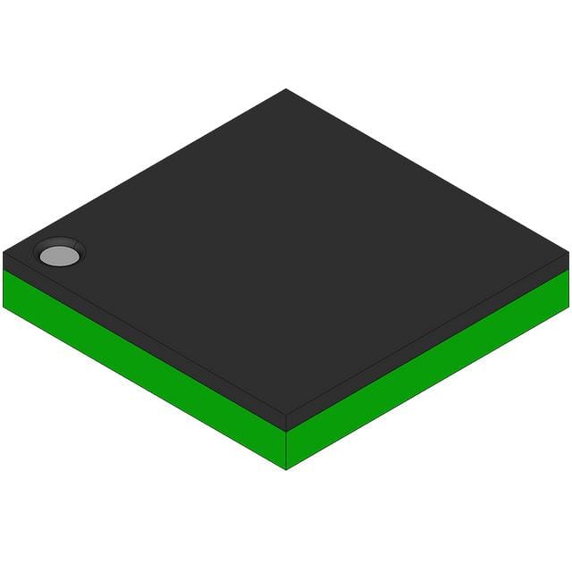
- Part No.:
- LM8333GGR8X/NOPB
- Manufacturer:
- Texas Instruments
- Category:
- Controllers
- Package:
- 49-TFBGA, CSPBGA
- Datasheet:
-
 LM8333GGR8X/NOPB.pdf
- Description:
- IC MOBILE I/O COMPANION 49-UARRA
- Quantity:
- Payment:

- Shipping:

Inventory:1,672
Please send an inquiry. Send us your inquiry, and we will respond immediately.
Product details
Overview
LM8333GGR8X/NOPB from Texas Instruments is a mobile I/O companion IC that offloads keyboard scanning and provides I/O expansion, PWM generation, and ACCESS.bus (I²C-compatible) host interface. It supports up to 72-key matrix (8×8 standard + 8 special-function keys), delivers <2 µA standby current, and features a 15-byte FIFO buffer with error reporting for key press/release events. It serves as a dedicated keypad controller in space-constrained portable devices.
For engineers reviewing the LM8333GGR8X/NOPB datasheet, LM8333GGR8X/NOPB pinout, LM8333GGR8X/NOPB application, or LM8333GGR8X/NOPB equivalent, this page details its verified keypad scanning architecture, programmable debounce/active timing, dual-interrupt-capable GPIOs, watchdog-integrated reset signaling, and WQFN-32 package implementation - all confirmed from TI's SNLS246K datasheet.
Technical Context
The LM8333GGR8X/NOPB implements a fully static architecture with hardware-managed Halt mode entry after configurable inactivity (default 500 ms), reducing current to <2 µA. Its internal RC oscillator (nominal 1 MHz, ±30% variation) drives keypad scanning at ~4 ms intervals and supports programmable debounce (1–255 × 3 ms) and active time (1–255 × 3 ms).
It operates as an I²C bus slave (7-bit address 0xA2/0xA3) compliant with ACCESS.bus at up to 400 kHz, with mandatory WD_OUT-to-RESET connection for watchdog functionality. Key event encoding uses MSB-set (press) / MSB-clear (release) 8-bit codes mapped to 8×8 matrix plus 8 SF-key positions, stored in a 15-byte FIFO with overrun detection.
Key Specifications
| Parameter | Value and Actual Design Meaning |
|---|---|
| Keypad Support | 8×8 matrix + 8 special-function keys = 72 total scannable keys; SF keys force WAKE_INx low and override same-row standard keys. |
| Standby Current | <2 µA in Halt mode; achieved by stopping internal RC clock when no keypad, I/O, or bus activity occurs. |
| FIFO Buffer | 15-byte depth; stores encoded key-press/release events (MSB=1/0) with automatic 0x00 termination; supports repeat-read without pointer advance. |
| I²C Interface | ACCESS.bus-compliant slave (address 0xA2 write / 0xA3 read); 400 kHz max speed; requires host-initiated transactions; NACK on first byte after wake-up. |
| PWM Capability | 16-bit programmable timer driving PWM pin; TLO/THI set via 0x40/0x41 commands; cycle time tC ≈ 1 µs; output configurable as push-pull, weak pull-up, or tri-state. |
| GPIO Pins | Four general-purpose I/Os (GEN_IO_0–GEN_IO_3); GEN_IO_0/GEN_IO_1 support edge-triggered external interrupts; all configurable as input (Hi-Z or weak pull-up) or output (drive high/low). |
| Operating Voltage | 2.25 V to 2.9 V; specified for -40°C to +85°C ambient; power-on reset triggered by supply rise time ≤10 ms. |
Pinout & Package
LM8333GGR8X/NOPB is packaged in a 32-pin WQFN (Package Number NJE0032A), 5 mm × 5 mm, 0.5 mm pitch, with exposed thermal pad. Pin functions are validated per TI SNLS246K Figure 1 and Signal Descriptions table.
| Pin/Terminal | Circuit Role | Design Meaning |
|---|---|---|
| WAKE_IN0–WAKE_IN7 | Keyboard scan inputs / SF-key wake sources | Eight dedicated inputs; SF keys pull these low to trigger wake-up and override standard key scanning in same row. |
| K_OUT0–K_OUT7 | Keyboard scan outputs | Eight column drivers for 8×8 matrix; actively driven during scanning cycles (~4 ms interval). |
| GEN_IO_0–GEN_IO_3 | Programmable bidirectional I/O | Configurable via GEN_IO_DIR/GEN_IO_OUT commands; GEN_IO_0/GEN_IO_1 support edge-triggered interrupts (SET_EXT_INT 0xD1). |
| SDA / SCL | I²C data / clock | Open-drain SDA, input-only SCL; supports 400 kHz ACCESS.bus; host must provide pull-ups. |
| IRQ | Interrupt request output | Active-low open-drain signal asserted on key events, errors, or enabled GPIO interrupts; cleared only by READ_INT (0xD0). |
| PWM | Programmable pulse-width modulated output | Driven by 16-bit timer; duty cycle set via PWM_HI/PWM_LO (0x40/0x41); also usable as general-purpose output. |
| WD_OUT | Watchdog timer output | Mandatory connection to system RESET; asserts low if watchdog not serviced; always enabled in hardware. |
| RESET | Asynchronous reset input | Active-low; resets internal state and FIFO; required to be connected to WD_OUT for proper watchdog operation. |
| CLK_IN | RC oscillator bias input | Connect to GND via 68 kΩ resistor to set nominal 1 MHz internal clock; tolerance ±30% over voltage/temperature. |
Key Features
| Feature | Design Value |
|---|---|
| Hardware-managed Halt mode | Enters sub-2 µA standby automatically after configurable inactivity; exited by keypad, GPIO, or I²C activity - no host polling required. |
| Dual-interrupt-capable GPIOs | GEN_IO_0 and GEN_IO_1 support rising/falling edge detection; generate IRQ and wake device from Halt mode; interrupt source identified in READ_INT code bits 1–2. |
| 72-key matrix encoding | Fixed 8×8 + 8 SF-key mapping with unique 8-bit codes (e.g., WAKE_IN0/K_OUT0 = 0x01); press/release distinguished by MSB; unambiguous for ≤2 simultaneous keys. |
| Configurable timing parameters | Debounce (1–255 × 3 ms) and active time (1–255 × 3 ms) programmed via DEBOUNCE (0x22) and ACTIVE (0xE4) commands - enables tuning for mechanical switch noise or system latency. |
| Integrated watchdog with hardwired reset | WD_OUT must connect to RESET; ensures system-level fault recovery without external components; eliminates need for discrete watchdog IC. |
Applications
| Mobile Phone Keypad Control | PDA Input Management |
|---|---|
Use Scenario: Managing physical keypad input in slim-profile GSM/UMTS handsets with limited MCU resources and strict battery life targets. IC Role / Device Role / Timing Role: Dedicated keypad scanner and I/O expander; handles 72-key matrix scanning, debouncing, and FIFO buffering independently of main processor. Use Value: Reduces host CPU load by >90% for key handling; extends battery life via <2 µA Halt-mode current; eliminates need for external debounce RC networks. | Use Scenario: Supporting stylus- and button-based navigation in legacy PDAs where MCU GPIOs are constrained and power budget is tight. IC Role / Device Role / Timing Role: I/O companion providing expandable GPIOs (GEN_IO_0–GEN_IO_3), programmable PWM backlight control, and reliable key-event buffering. Use Value: Enables reuse of aging MCU designs by adding 4 flexible I/Os and 1 PWM channel; supports slow-edge interrupts for tactile button wake-up without MCU polling. |
| Smart Handheld Media Player UI | Portable Gaming Device Input |
Use Scenario: Handling multi-function buttons (play/pause/volume/menu) and jog-dial inputs in flash-based media players with OLED displays. IC Role / Device Role / Timing Role: Centralized input manager interfacing with host via I²C; decodes key events and routes them via IRQ; drives PWM-controlled LED indicators. Use Value: Provides deterministic 4-ms scan timing and 15-byte FIFO depth to prevent missed rapid key sequences during playback control. | Use Scenario: Scanning directional pads, action buttons, and shoulder triggers in handheld game consoles requiring low-latency, glitch-free input capture. IC Role / Device Role / Timing Role: Keypad controller with error detection (KEYOVR flag for >2-key press) and fast IRQ assertion (<10 µs propagation) to minimize input lag. Use Value: Prevents ambiguous multi-key states via hardware KEYOVR flag and FIFO overflow reporting; ensures consistent response during fast-paced gameplay. |
Equivalent & Alternatives
The following parts are listed as comparable options for similar keypad controller and I/O expansion applications.
| Alternative Part | Technical Difference | Application Difference | Selection Advice |
|---|---|---|---|
| TCA6408A | 8-bit I/O expander only; no keypad scanning, FIFO, or PWM; I²C address selectable (0x20–0x27); no watchdog or WAKE_IN inputs. | Suitable for simple GPIO extension but cannot replace LM8333GGR8X/NOPB's integrated key-scan logic or SF-key wake capability. | Select when only basic I/O expansion is needed and host handles all scanning/debouncing in firmware. |
| MAX7317 | 16-bit I/O expander with interrupt output; supports key-scan mode (8×8) but lacks SF-keys, WD_OUT, and programmable active/debounce timing; no FIFO buffer. | Provides key-scan assist but requires host to poll registers for events; no hardware error reporting for multi-key press or FIFO overrun. | Choose for cost-sensitive designs needing basic scan assist without advanced power management or error resilience. |
Compared with TCA6408A and MAX7317, LM8333GGR8X/NOPB uniquely integrates hardware-accelerated 72-key scanning, 15-byte FIFO buffering, mandatory watchdog reset signaling, and dual-edge GPIO interrupts - enabling lower host firmware overhead and higher reliability in battery-powered handhelds.
Availability
LM8333GGR8X/NOPB is available at Aetrix Electronics and suitable for mobile phones, personal digital assistants (PDAs), smart handheld devices, and personal media players requiring stable component supply and long-term lifecycle support.
Supply support for LM8333GGR8X/NOPB includes scheduled delivery planning, volume procurement assistance, BOM continuity management, traceable sourcing, and lifecycle availability coordination for OEM customers, industrial embedded developers, connected-device designers, and electronics production programs.
Manufacturer
Texas Instruments is a global semiconductor company headquartered in Dallas, Texas, delivering analog and embedded processing solutions across industrial, automotive, and personal electronics markets.
The LM8333 product line was designed specifically for ultra-low-power mobile I/O management, integrating keypad scanning, GPIO expansion, PWM generation, and watchdog functionality into a single chip-scale package for space- and power-constrained portable devices.
FAQ
What is the function of the WD_OUT pin on the LM8333GGR8X/NOPB?
The WD_OUT pin on the LM8333GGR8X/NOPB is the watchdog timer output and must be connected directly to the system RESET input. It is always enabled in hardware and asserts low if the watchdog is not serviced, ensuring fail-safe system recovery. This eliminates the need for an external watchdog IC and guarantees deterministic reset behavior during firmware hangs or initialization failures.
How does the LM8333GGR8X/NOPB handle simultaneous key presses?
The LM8333GGR8X/NOPB detects and reports simultaneous key presses beyond two via the KEYOVR error flag in the error code register (READ_ERROR command 0xF0). When more than two keys are pressed, the resulting matrix pattern becomes ambiguous, so the device asserts IRQ and sets KEYOVR - alerting the host to discard or reinterpret the FIFO contents. This prevents misinterpretation of user input in dense keypad layouts.
Can the LM8333GGR8X/NOPB operate without an external crystal or clock source?
Yes, the LM8333GGR8X/NOPB operates autonomously using its internal RC oscillator. The CLK_IN pin requires only a 68 kΩ resistor to ground to bias the oscillator at ~1 MHz (±30% over voltage and temperature). No external crystal, clock generator, or timing component is needed - simplifying BOM and PCB layout while maintaining sufficient accuracy for keypad scanning.
What is the purpose of the WAKE_IN pins on the LM8333GGR8X/NOPB?
The eight WAKE_IN pins (WAKE_IN0–WAKE_IN7) on the LM8333GGR8X/NOPB serve dual roles: as keyboard scan inputs for the 8×8 matrix and as dedicated wake-up sources for special-function (SF) keys. Pressing an SF key pulls its assigned WAKE_IN pin low, forcing immediate wake-up from Halt mode and overriding any standard key in the same row - enabling priority input handling without host intervention.
Is the LM8333GGR8X/NOPB pin-compatible with other members of the LM8333 family?
No, LM8333GGR8X/NOPB is the 32-pin WQFN variant (NJE0032A package); it is not pin-compatible with the 49-ball csBGA version (NYC0049A). Pin assignments differ significantly between packages - e.g., WAKE_IN0 is pin 29 in WQFN but pin D7 in csBGA. Migration requires PCB redesign; functional compatibility exists, but mechanical and electrical layout is not interchangeable.
LM8333GGR8X/NOPB Specifications
- Product attributes
- Attribute value
- Manufacturer:
- Texas Instruments
- Package/Case:
- 49-TFBGA, CSPBGA
- Programmable:
- Not Verified
- Protocol:
- -
- Function:
- Controller
- Interface:
- ACCESS.bus, I2C
- Standards:
- -
- Voltage - Supply:
- 2.25V ~ 2.9V
- Current - Supply:
- 6mA
- Operating Temperature:
- -40°C ~ 85°C
- Supplier Device Package:
- 49-CSBGA (4x4)
- Grade:
- -
- Qualification:
- -
LM8333GGR8X/NOPB FAQ
1.How can I place an order for LM8333GGR8X/NOPB through Aetrix?
Please submit a Request for Quotation (RFQ) for LM8333GGR8X/NOPB on Aetrix. Our sales agent will provide a competitive quotation and guide you through the order confirmation once you accept the terms.
2.Are the price and stock information for LM8333GGR8X/NOPB reliable?
The price and inventory of LM8333GGR8X/NOPB are updated periodically and may fluctuate due to market conditions. Stock and pricing data are typically refreshed every 24 hours. Quotation validity for LM8333GGR8X/NOPB is usually 5 days.
3.What payment methods are accepted for LM8333GGR8X/NOPB?
We accept Wire Transfer, PayPal, Credit Card, Western Union, MoneyGram, and Escrow for LM8333GGR8X/NOPB transactions.
Note: Certain payment methods may incur a processing fee.
4.How is shipping managed for LM8333GGR8X/NOPB?
LM8333GGR8X/NOPB orders can be shipped via leading logistics carriers, including DHL, UPS, FedEx, TNT, or Registered Mail.
Once your LM8333GGR8X/NOPB order is processed, you will receive an email with the shipment details and tracking number.
Note: Tracking information may take up to 24 hours to appear. Express delivery typically takes 3–5 business days.
5.How can I obtain technical support or documentation for LM8333GGR8X/NOPB?
For technical support, including LM8333GGR8X/NOPB datasheets, pinout diagrams, or application guidance, please contact our engineering support team. They can provide detailed documentation and assistance for your LM8333GGR8X/NOPB requirements.
6.How does Aetrix verify that LM8333GGR8X/NOPB is sourced from the original manufacturer or authorized distributors?
All LM8333GGR8X/NOPB products on Aetrix are procured from qualified distributors and authorized channels. Our dedicated quality assurance team conducts strict verification, including traceability checks and, if necessary, third-party testing. This ensures that LM8333GGR8X/NOPB meets industry standards.
7.What is the process for return or replacement of LM8333GGR8X/NOPB?
All LM8333GGR8X/NOPB units undergo pre-shipment inspection (PSI). If there is an issue with LM8333GGR8X/NOPB, returns or replacements are accepted under the following conditions:
1.Quantity discrepancies, incorrect items, or visible external defects (such as breakage or corrosion), acknowledged by Aetrix.
2.The issue is reported within 90 days of delivery.
3.The LM8333GGR8X/NOPB part is unused and in its original packaging.
Return procedure for LM8333GGR8X/NOPB:
1.Submit a request within 90 days.
2.Obtain a Return Material Authorization (RMA) from Aetrix.
LM8333GGR8X/NOPB Tags

-
PTN5150AHXMP
NXP Semiconductors

-
USB3740B-AI9-TR
Microchip Technology

-
USB3740B-AI2-TR
Microchip Technology

-
USB3300-EZK-TR
Microchip Technology
-
USB3300-EZK
Microchip Technology

-
FUSB340TMX
onsemi

-
FUSB302BMPX
onsemi

-
DP83826IRHBR
Texas Instruments

-
MCP2518FDT-E/QBB
Microchip Technology
-
FUSB302MPX
onsemi

-
MCP2518FDT-E/SL
Microchip Technology

-
FT260Q-R
FTDI, Future Technology Devices International Ltd
Tech Hub

A practical engineering guide to 3.3V and 5V logic compatibility, input thresholds, resistor dividers, translator ICs, MOSFET level shifting, I2C pull-ups, timing limits and power-sequencing risks.

The 74HC595 uses push-pull logic outputs, while the TPIC6B595 uses 50 V open-drain DMOS sinks for higher-power loads. This guide compares timing, current limits, 3.3 V interfacing, load wiring, thermal…

The 74HC595 converts serial data into eight stable parallel outputs. This guide covers pin functions, shift and storage timing, OE and MR behavior, drive-current limits, cascading, voltage compatibilit…

A technical comparison of level-sensitive latches and edge-triggered flip-flops, covering timing windows, setup and hold limits, master–slave operation, time borrowing, race-through, HDL inference and…

A D latch stores one bit while Enable controls when data can pass. This reference covers gate-level operation, truth tables, transparency, setup and hold timing, LE versus OE, common ICs and practical …

An SR latch stores one bit through cross-coupled feedback. This engineering reference covers NOR and NAND implementations, truth tables, forbidden-state recovery, gated operation, switch debouncing, fa…

Latch circuits retain one bit through feedback. This technical reference covers SR and D latches, truth tables, transparency, timing limits, latch-versus-flip-flop behavior, applications and common log…

An engineering guide to LED driver operation, constant-current and constant-voltage outputs, linear and switching topologies, dimming, IC selection, calculations, replacement compatibility, and fault c…

Operational amplifier guide covering op amp basics, feedback, ideal vs real op amps, common configurations, buffer circuits, offset, bias current, gain-bandwidth, slew rate, rail-to-rail limits and sel…

Jumper cables guide covering safe connection order, red and black clamp placement, final ground connection, cable gauge, length, clamp quality, copper vs CCA cables, jump starter comparison and battery…


