
 My Inquiry
 My Account


Texas Instruments LMH0071SQ/NOPB
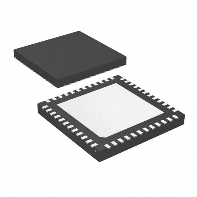
- Part No.:
- LMH0071SQ/NOPB
- Manufacturer:
- Texas Instruments
- Category:
- Serializers, Deserializers
- Package:
- 48-WFQFN Exposed Pad
- Datasheet:
-
 LMH0071SQ/NOPB.pdf
- Description:
- IC DESERIAL SDI W/LVDS 48WQFN
- Quantity:
- Payment:

- Shipping:

Inventory:279
Please send an inquiry. Send us your inquiry, and we will respond immediately.
Product details
Overview
LMH0071SQ/NOPB from Texas Instruments is a 3 Gbps SDI deserializer with integrated SMPTE-compliant reclocked loopthrough cable driver, 5-bit LVDS output interface, and SMBus configuration. It supports SMPTE 259M-C (SD), SMPTE 292M (HD), and SMPTE 424M (3G) standards, operates from −40°C to +85°C, and targets video camera and broadcast infrastructure applications requiring robust serial digital signal recovery.
For engineers reviewing the LMH0071SQ/NOPB datasheet, LMH0071SQ/NOPB pinout, LMH0071SQ/NOPB application, or LMH0071SQ/NOPB equivalent, this device delivers deterministic jitter tolerance (0.6 UI min), programmable LVDS swing, dual differential serial inputs (RXIN0/RXIN1), DVB-ASI mode support, and loopthrough enable control-key selection criteria for SDI receiver design in professional video systems.
Technical Context
The LMH0071SQ/NOPB implements a CDR-based architecture that autonomously detects incoming data rates (270 Mbps–2.97 Gbps) and recovers embedded clock without external VCO. Its internal PLL uses an external R-C loop filter (LF_CP/LF_REF pins) and achieves lock acquisition in ≤24 ms after reset or rate change.
It features a 2:1 input multiplexer (RX_MUX_SEL controlled), bypassable 8b10b decode (DVB_ASI pin-selectable), and a current-mode CML loopthrough output (TXOUT±) compliant with SMPTE 259M/292M/424M return loss and amplitude requirements when terminated to 2.5V.
Key Specifications
| Parameter | Value and Actual Design Meaning |
|---|---|
| Data Rate Support | 270 Mbps, 1.485 Gbps, and 2.97 Gbps - enables single-device compatibility across SD, HD, and 3G-SDI video links. |
| Input Jitter Tolerance | 0.6 UI minimum - ensures reliable lock under SMPTE RP184-compliant jitter conditions at 3G rate. |
| LVDS Output Swing | 230–310 mV differential - meets ANSI/TIA/EIA-644 for low-noise FPGA interfacing over ≤25 cm traces. |
| Power Dissipation | 532–710 mW - varies with data rate and loopthrough state; typical 590 mW at 3G with loopthrough disabled. |
| Operating Temperature | −40°C to +85°C - qualified for industrial-grade broadcast equipment deployment. |
| SMBus Interface | 10–100 kHz, 3.3V LVCMOS - enables register-level configuration (e.g., output timing, DVB-ASI mode, GPIO setup). |
| Loopthrough Output | 720–880 mV into 75 Ω - SMPTE-compliant amplitude with automatic slew-rate adaptation per data rate. |
Pinout & Package
LMH0071SQ/NOPB is housed in a 48-pin WQFN package (7 mm × 7 mm, 0.5 mm pitch) with exposed thermal pad (DAP = GND). Pin assignments are validated per TI SNLS272Q Rev. April 2013.
| Pin/Terminal | Circuit Role | Design Meaning |
|---|---|---|
| RXIN0± | Differential Serial Input Channel 0 | Primary SDI input path; selected when RX_MUX_SEL = L; supports all supported data rates. |
| RXIN1± | Differential Serial Input Channel 1 | Secondary SDI input; selected when RX_MUX_SEL = H; enables source switching without external mux. |
| TXOUT± | CML Loopthrough Output | Reclocked, SMPTE-compliant serial output; requires 75 Ω termination to VDD2V5 for 720–880 mV amplitude. |
| RX[4:0]±, RXCLK± | 5-Bit DDR LVDS Output Bus | Parallel video data and clock to FPGA; 100 Ω differential termination required; tDVBC/tDVAC < 650 ps timing margin. |
| LOCK, RESET | PLL Status & Hardware Reset | LOCK = L indicates stable CDR lock; RESET = L forces full hardware initialization including register defaults. |
| DVB_ASI, Loopthru_EN | Mode & Function Enable | DVB_ASI = H activates 8b10b decode and idle-character detection on RX4; Loopthru_EN = H enables TXOUT± output. |
Key Features
| Feature | Design Value |
|---|---|
| No external VCO or clock required | Integrated CDR with auto-rate detection eliminates timing component count and board space for reference clocks. |
| Reclocked serial loopthrough with cable driver | TXOUT± provides SMPTE-compliant output with adaptive slew rate-enables daisy-chain or monitoring without external driver IC. |
| Bypassable 8b10b decode | DVB_ASI pin selects between raw bitstream (L) and decoded nibble + idle flag (H), simplifying integration with ASI transport layer logic. |
| 5-bit LVDS interface to FPGA | DDR LVDS outputs reduce pin count vs. single-ended parallel interfaces while maintaining noise immunity and timing margins. |
| Industrial temperature range | −40°C to +85°C operation ensures reliability in uncontrolled broadcast environments like field cameras and mobile trucks. |
Applications
| Video Cameras | DVRs |
|---|---|
Use Scenario: Capturing uncompressed HD/3G-SDI video streams from CMOS sensors for real-time encoding and storage. IC Role / Device Role / Timing Role: Deserializes incoming SMPTE 292M/424M signal, reclocks it, and delivers parallel LVDS data to FPGA-based image processing pipeline. Use Value: Enables direct sensor-to-FPGA interface with <650 ps data-to-clock skew, eliminating need for external clock clean-up or level-shifting. | Use Scenario: Receiving multi-channel SDI feeds in broadcast-grade digital video recorders for simultaneous recording and playback. IC Role / Device Role / Timing Role: Provides synchronized, jitter-cleaned LVDS outputs to memory controller; loopthrough supports feed-through to monitoring outputs. Use Value: 0.6 UI input jitter tolerance ensures error-free capture of degraded long-cable SDI signals common in studio routing. |
| Video Switchers | Video Editing Systems |
Use Scenario: Routing multiple SDI sources in live production switchers with minimal latency and frame sync integrity. IC Role / Device Role / Timing Role: Acts as input receiver with 2:1 mux (RX_MUX_SEL) for seamless source switching; LOCK pin signals lock status to system controller. Use Value: ≤24 ms link acquisition time allows sub-frame switching without visible glitches during live cuts. | Use Scenario: Ingesting high-bitrate 3G-SDI footage into non-linear editing workstations for color grading and effects rendering. IC Role / Device Role / Timing Role: Converts serial baseband video to parallel LVDS for FPGA-accelerated de-embedding, metadata extraction, and format conversion. Use Value: SMBus-configurable LVDS timing (register 0x28h) enables precise alignment with FPGA capture logic across varying board delays. |
Equivalent & Alternatives
The following parts are listed as comparable options for similar SDI deserializer applications.
| Alternative Part | Technical Difference | Application Difference | Selection Advice |
|---|---|---|---|
| LMH0041SQ/NOPB | Supports up to 1.485 Gbps only; no SMPTE 424M (3G) compliance; identical pinout and SMBus interface. | Limited to HD-SDI; unsuitable for 3G-SDI camera backends or 1080p60+ workflows. | Select LMH0041SQ/NOPB only when cost-sensitive HD-only designs do not require 3G capability. |
| LMH0341SQ/NOPB | Full 3G-SDI support (2.97 Gbps); adds active loopthrough with cable driver; same 48-pin WQFN package. | Enables reclocked distribution to downstream devices; supports higher-jitter 3G sources via enhanced CDR architecture. | Choose LMH0341SQ/NOPB when loopthrough functionality and maximum jitter tolerance are required in 3G systems. |
Compared with LMH0041SQ/NOPB, LMH0071SQ/NOPB adds 3G-SDI support but omits active loopthrough; compared with LMH0341SQ/NOPB, it retains identical loopthrough capability but lacks the enhanced CDR jitter handling of the LMH0341, making it optimal for cost-constrained 3G-SDI receivers where loopthrough is needed but extreme jitter resilience is not.
Availability
LMH0071SQ/NOPB is available at Aetrix Electronics and suitable for video cameras, DVRs, video switchers, and video editing systems requiring stable component supply for broadcast infrastructure programs.
Supply support for LMH0071SQ/NOPB includes scheduled delivery planning, volume procurement assistance, BOM continuity management, traceable sourcing, and lifecycle availability coordination for OEM customers, industrial embedded developers, connected-device designers, and electronics production programs.
Manufacturer
Texas Instruments is a global semiconductor company delivering analog and embedded processing solutions for industrial, automotive, and communications markets.
The LMH0071SQ/NOPB belongs to TI's FPGA-Attach SER/DES product line, designed specifically for high-reliability SDI video signal reception in professional broadcast equipment with minimal external components.
FAQ
What video standards does the LMH0071SQ/NOPB support?
The LMH0071SQ/NOPB supports SMPTE 259M-C (SD-SDI), SMPTE 292M (HD-SDI), and SMPTE 424M (3G-SDI) standards, plus DVB-ASI mode for transport stream decoding. It automatically detects data rates from 270 Mbps to 2.97 Gbps and configures its CDR and loopthrough driver accordingly. This makes LMH0071SQ/NOPB suitable for multi-standard broadcast gear without firmware changes.
Does the LMH0071SQ/NOPB require an external clock or VCO?
No, the LMH0071SQ/NOPB does not require an external clock or VCO. Its integrated CDR recovers clock directly from the incoming SDI data stream and generates a clean, reclocked output (RXCLK±) for the host FPGA. The LMH0071SQ/NOPB achieves autonomous lock acquisition in ≤24 ms after power-up or input rate change, eliminating timing component dependencies.
How is the loopthrough function enabled on the LMH0071SQ/NOPB?
The loopthrough function on the LMH0071SQ/NOPB is enabled by driving the Loopthru_EN pin high. When asserted, the device routes the reclocked serial data to TXOUT± outputs with SMPTE-compliant amplitude (720–880 mV) and slew rate. TXOUT± must be terminated with 75 Ω to VDD2V5; disabling Loopthru_EN (pin low) powers down the output driver to reduce power consumption in LMH0071SQ/NOPB systems not requiring feed-through.
What is the purpose of the DVB_ASI pin on the LMH0071SQ/NOPB?
The DVB_ASI pin on the LMH0071SQ/NOPB selects between standard SDI deserialization (DVB_ASI = L) and DVB-ASI transport stream mode (DVB_ASI = H). In DVB-ASI mode, the LMH0071SQ/NOPB performs 8b10b decoding, presenting nibble-aligned data on RX[3:0] and idle-character detection on RX4. This enables direct interface to ASI demux logic without external decode IP, reducing FPGA resource usage in broadcast encoders.
What are the power supply requirements for the LMH0071SQ/NOPB?
The LMH0071SQ/NOPB requires two supplies: 3.3 V (VDD3V3, VDDPLL) and 2.5 V (VDD2V5). VDD3V3 powers core logic and LVDS outputs; VDDPLL supplies the PLL circuitry and requires a 22 μF capacitor; VDD2V5 powers the loopthrough output stage and SMBus I/O. TI specifies sequencing-3.3 V must be applied before 2.5 V-and recommends 4.7 μF + 0.1 μF bypassing per supply pin. The DAP (exposed pad) must be soldered to GND for thermal and electrical integrity in LMH0071SQ/NOPB layouts.
LMH0071SQ/NOPB Specifications
- Product attributes
- Attribute value
- Manufacturer:
- Texas Instruments
- Series:
- -
- Package/Case:
- 48-WFQFN Exposed Pad
- Packaging:
- Tape & Reel (TR)
- Product Status:
- Active
- Function:
- Deserializer
- Data Rate:
- 2.97Gbps
- Input Type:
- LVCMOS
- Output Type:
- LVDS
- Number of Inputs:
- 2
- Number of Outputs:
- 5
- Voltage - Supply:
- 2.5V, 3.3V
- Operating Temperature:
- -40°C ~ 85°C (TA)
- Grade:
- -
- Qualification:
- -
- Mounting Type:
- Surface Mount
- Supplier Device Package:
- 48-WQFN (7x7)
LMH0071SQ/NOPB FAQ
1.How can I place an order for LMH0071SQ/NOPB through Aetrix?
Please submit a Request for Quotation (RFQ) for LMH0071SQ/NOPB on Aetrix. Our sales agent will provide a competitive quotation and guide you through the order confirmation once you accept the terms.
2.Are the price and stock information for LMH0071SQ/NOPB reliable?
The price and inventory of LMH0071SQ/NOPB are updated periodically and may fluctuate due to market conditions. Stock and pricing data are typically refreshed every 24 hours. Quotation validity for LMH0071SQ/NOPB is usually 5 days.
3.What payment methods are accepted for LMH0071SQ/NOPB?
We accept Wire Transfer, PayPal, Credit Card, Western Union, MoneyGram, and Escrow for LMH0071SQ/NOPB transactions.
Note: Certain payment methods may incur a processing fee.
4.How is shipping managed for LMH0071SQ/NOPB?
LMH0071SQ/NOPB orders can be shipped via leading logistics carriers, including DHL, UPS, FedEx, TNT, or Registered Mail.
Once your LMH0071SQ/NOPB order is processed, you will receive an email with the shipment details and tracking number.
Note: Tracking information may take up to 24 hours to appear. Express delivery typically takes 3–5 business days.
5.How can I obtain technical support or documentation for LMH0071SQ/NOPB?
For technical support, including LMH0071SQ/NOPB datasheets, pinout diagrams, or application guidance, please contact our engineering support team. They can provide detailed documentation and assistance for your LMH0071SQ/NOPB requirements.
6.How does Aetrix verify that LMH0071SQ/NOPB is sourced from the original manufacturer or authorized distributors?
All LMH0071SQ/NOPB products on Aetrix are procured from qualified distributors and authorized channels. Our dedicated quality assurance team conducts strict verification, including traceability checks and, if necessary, third-party testing. This ensures that LMH0071SQ/NOPB meets industry standards.
7.What is the process for return or replacement of LMH0071SQ/NOPB?
All LMH0071SQ/NOPB units undergo pre-shipment inspection (PSI). If there is an issue with LMH0071SQ/NOPB, returns or replacements are accepted under the following conditions:
1.Quantity discrepancies, incorrect items, or visible external defects (such as breakage or corrosion), acknowledged by Aetrix.
2.The issue is reported within 90 days of delivery.
3.The LMH0071SQ/NOPB part is unused and in its original packaging.
Return procedure for LMH0071SQ/NOPB:
1.Submit a request within 90 days.
2.Obtain a Return Material Authorization (RMA) from Aetrix.
LMH0071SQ/NOPB Tags

-
SN65HVS880PWPR
Texas Instruments
-
SN65HVS882PWPR
Texas Instruments

-
FIN3386MTDX
onsemi
-
FIN3385MTDX
onsemi

-
SN65LV1023ARHBR
Texas Instruments

-
SN65LV1023ADBR
Texas Instruments
-
SN65LV1224BDBR
Texas Instruments

-
SN65LVDS93ADGGR
Texas Instruments
-
SN65LVDS93DGGR
Texas Instruments

-
TDES954RGZT
Texas Instruments
-
SN65LV1224BRHBT
Texas Instruments

-
DS90UB914QSQE/NOPB
Texas Instruments
Tech Hub

A practical engineering guide to 3.3V and 5V logic compatibility, input thresholds, resistor dividers, translator ICs, MOSFET level shifting, I2C pull-ups, timing limits and power-sequencing risks.

The 74HC595 uses push-pull logic outputs, while the TPIC6B595 uses 50 V open-drain DMOS sinks for higher-power loads. This guide compares timing, current limits, 3.3 V interfacing, load wiring, thermal…

The 74HC595 converts serial data into eight stable parallel outputs. This guide covers pin functions, shift and storage timing, OE and MR behavior, drive-current limits, cascading, voltage compatibilit…

A technical comparison of level-sensitive latches and edge-triggered flip-flops, covering timing windows, setup and hold limits, master–slave operation, time borrowing, race-through, HDL inference and…

A D latch stores one bit while Enable controls when data can pass. This reference covers gate-level operation, truth tables, transparency, setup and hold timing, LE versus OE, common ICs and practical …

An SR latch stores one bit through cross-coupled feedback. This engineering reference covers NOR and NAND implementations, truth tables, forbidden-state recovery, gated operation, switch debouncing, fa…

Latch circuits retain one bit through feedback. This technical reference covers SR and D latches, truth tables, transparency, timing limits, latch-versus-flip-flop behavior, applications and common log…

An engineering guide to LED driver operation, constant-current and constant-voltage outputs, linear and switching topologies, dimming, IC selection, calculations, replacement compatibility, and fault c…

Operational amplifier guide covering op amp basics, feedback, ideal vs real op amps, common configurations, buffer circuits, offset, bias current, gain-bandwidth, slew rate, rail-to-rail limits and sel…

Jumper cables guide covering safe connection order, red and black clamp placement, final ground connection, cable gauge, length, clamp quality, copper vs CCA cables, jump starter comparison and battery…


