
 My Inquiry
 My Account


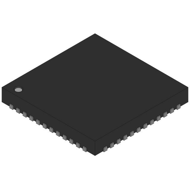
Texas Instruments LMH0356SQ/NOPB
- Part No.:
- LMH0356SQ/NOPB
- Manufacturer:
- Texas Instruments
- Category:
- Video Processing
- Package:
- 48-WFQFN Exposed Pad
- Datasheet:
-
 LMH0356SQ/NOPB.pdf
- Description:
- IC VIDEO RECLOCKER 48WQFN
- Quantity:
- Payment:

- Shipping:

Inventory:1,541
Please send an inquiry. Send us your inquiry, and we will respond immediately.
Product details
Overview
LMH0356SQ/NOPB from Texas Instruments is a 3-Gbps HD/SD SDI reclocker with integrated 4:1 input multiplexer and four independent FR4 equalizers, supporting SMPTE ST-424 (2.97 Gbps), ST-292 (1.485 Gbps), ST-259 (270 Mbps), and DVB-ASI (270 Mbps). It provides two differential LVPECL-compatible outputs - one fixed retimed data output (SDO) and one configurable output (SCO/SDO2) selectable as either second retimed data or low-jitter recovered clock - and operates from a single 3.3-V supply with 430-mW typical power consumption in active mode.
For engineers reviewing the LMH0356SQ/NOPB datasheet, LMH0356SQ/NOPB pinout, LMH0356SQ/NOPB application, or LMH0356SQ/NOPB equivalent, key selection considerations include its auto-rate detection across five video data rates, 0–30-inch FR4 trace equalization per input, lock-detect and SD/HD rate indicator outputs, LVCMOS control interface, and dual-package availability (40-pin and 48-pin WQFN) with footprint compatibility to LMH0056/LMH0036.
Technical Context
The LMH0356SQ/NOPB implements a PLL-based reclocking architecture with VCO and dual loop filters (LF1/LF2) for jitter suppression across SD, HD, and 3G-SDI data streams. Its 4:1 input mux selects among four differential CML/LVPECL inputs (SDI0–SDI3), each equipped with an adaptive FR4 equalizer that requires no configuration for trace lengths up to 30 inches.
Control logic enables manual or automatic bypass modes, output mute, SCO/SDO2 function selection (data vs. recovered clock), and rate locking indication via LOCK DETECT and SD/HD outputs. The device uses a 27-MHz crystal or external reference (XTAL IN/EXT CLK) and supports both auto-rate detection and manual RATE[1:0] programming for deterministic operation at 270/1483/1485/2967/2970 Mbps.
Key Specifications
| Parameter | Value and Actual Design Meaning |
|---|---|
| Data Rates | 270 Mbps, 1.483 Gbps, 1.485 Gbps, 2.967 Gbps, 2.97 Gbps - covers SMPTE ST-259/ST-292/ST-424 and DVB-ASI standards |
| Input Equalization | 0–30 inches of FR4 trace per channel - eliminates need for external equalizers or configuration registers |
| Output Jitter | 0.03 UIP-P @ 270 Mbps, 0.05 UIP-P @ 1.485 Gbps, 0.09 UIP-P @ 2.97 Gbps - meets SMPTE jitter compliance for broadcast-grade retiming |
| Power Supply | Single 3.3-V supply (±5%) - simplifies system power architecture; 430-mW typical active power, 10-mW in power-down mode |
| Interface Compatibility | Differential CML/LVPECL I/O, LVCMOS control - interoperable with TI's LMH0344 (EQ), LMH0302 (driver), and standard SDI PHYs |
| Operating Temperature | –40°C to +85°C - qualified for industrial and broadcast equipment environments |
| Package | 40-pin WQFN (5.0 mm × 5.0 mm) - space-efficient footprint compatible with LMH0056/LMH0036 layout |
Pinout & Package
LMH0356SQ/NOPB is packaged in a 40-pin WQFN (RSB) with 5.0 mm × 5.0 mm body size and exposed die attach pad electrically connected to VEE (ground). The pad must be soldered to a PCB ground plane for thermal and electrical integrity.
| Pin/Terminal | Circuit Role | Design Meaning |
|---|---|---|
| SDI0–SDI3 (True/Complement) | Differential serial data inputs | Four independent CML/LVPECL-compatible inputs with internal 50-Ω termination; each supports 0–30-inch FR4 equalization |
| SDO (True/Complement) | Primary retimed serial data output | Differential LVPECL-compatible output; 750 mVP-P into 100-Ω load; always active when enabled |
| SCO/SDO2 (True/Complement) | Configurable secondary output | Selectable via SCO_EN as second retimed data output or low-jitter recovered clock (270/1485/2970 MHz) |
| LOCK DETECT | PLL lock status indicator | Active-high open-drain LVCMOS output; asserts within 15 ms of valid signal acquisition; drives OUTPUT MUTE |
| SD/HD | Data rate range indicator | LVCMOS output high = 270 Mbps (SD), low = ≥1.483 Gbps (HD/3G); registered and valid only when PLL locked |
| ENABLE | Global device enable | LVCMOS input with internal pullup; pulls device into 10-mW power-down state when low; XTAL circuit remains active |
| SEL0/SEL1 | Input channel select | LVCMOS inputs with internal pulldowns; encode 4:1 mux selection (00=SDI0, 01=SDI1, 10=SDI2, 11=SDI3) |
| RATE0/RATE1 | Manual data rate select | LVCMOS inputs with internal pulldowns; configure fixed-rate mode (01=270 Mbps, 10=1.485/2.97 Gbps) or auto-detect (00) |
| BYPASS/AUTO BYPASS | Reclocking mode control | LVCMOS input with internal pulldown; high = forced bypass, low = auto-bypass on unlock or unsupported rate |
| OUTPUT MUTE | Output disable control | LVCMOS input with internal pullup; low = mutes SDO and SCO/SDO2 simultaneously; overrides bypass mode |
| XTAL IN/EXT CLK | Timing reference input | Accepts 27-MHz parallel-resonant crystal or LVCMOS clock; required for PLL operation and rate recovery |
| XTAL OUT | Crystal oscillator output | Drives external crystal; enables daisy-chaining reference clocks to multiple reclockers in multi-channel systems |
| LF1/LF2 | PLL loop filter connections | Analog nodes for external RC filter components; set loop bandwidth (275 kHz to 2.75 MHz) per data rate |
| VCC / VEE | Power supply terminals | VCC = 3.3 V (7 pins), VEE = ground (6 pins + exposed pad); decoupling required per TI layout guidelines |
Key Features
| Feature | Design Value |
|---|---|
| 4:1 Input Multiplexer with Per-Channel FR4 EQ | Enables flexible routing of four SDI sources without external switching or equalization ICs; eliminates board-level tuning |
| Auto-Rate Detection & Manual Rate Select | Supports seamless transition between SD/HD/3G-SDI formats while allowing deterministic lock behavior in fixed-rate systems |
| Dual Differential Outputs with SCO/SDO2 Flexibility | Provides either second retimed data path or recovered clock output - critical for clock distribution in routers and switchers |
| Integrated Lock Detect and SD/HD Indicator | Enables real-time status monitoring and downstream device coordination (e.g., enabling LMH0302 driver gain based on rate) |
| Low-Power Power-Down Mode | Reduces system standby power to 10 mW while preserving XTAL reference for cascaded reclockers - improves thermal management |
| Footprint-Compatible Upgrade Path | 40-pin WQFN layout matches LMH0056/LMH0036 - allows drop-in migration to higher data rate capability without PCB redesign |
Applications
| Digital Video Router | Video Format Converter |
|---|---|
Use Scenario: Receiving and redistributing multiple SDI feeds across a matrix switcher with long backplane traces. IC Role / Device Role / Timing Role: Reclocker with integrated 4:1 mux and FR4 equalization - cleans jitter accumulated over FR4 interconnects and selects active source. Use Value: Enables reliable 3G-SDI distribution over >20-inch PCB traces without external equalizers or clock cleaners. |
Use Scenario: Converting between SD-SDI (270 Mbps), HD-SDI (1.485 Gbps), and 3G-SDI (2.97 Gbps) signals in broadcast production gear. IC Role / Device Role / Timing Role: Rate-adaptive retimer - detects incoming data rate and retransmits clean, low-jitter output at same rate with SD/HD flag for downstream processing. Use Value: Eliminates need for separate reclockers per standard; single IC handles all SMPTE-compliant video rates. |
| DVB-ASI Equipment | Professional Video Editing System |
Use Scenario: Retiming MPEG-2 transport streams over coaxial cable in satellite contribution links. IC Role / Device Role / Timing Role: DVB-ASI compliant reclocker - locks to 270-Mbps 8B10B-encoded data without harmonic interference. Use Value: Maintains bit-error-free transmission through legacy infrastructure with degraded signal integrity. |
Use Scenario: Synchronizing multi-channel video capture cards in non-linear editing workstations. IC Role / Device Role / Timing Role: Jitter-suppressing reclocker with recovered clock output - provides low-phase-noise timing reference for ADC sampling clocks. Use Value: Reduces timing skew between channels, improving frame alignment accuracy during multi-camera ingest. |
Equivalent & Alternatives
The following parts are listed as comparable options for similar SDI reclocking applications.
| Alternative Part | Technical Difference | Application Difference | Selection Advice |
|---|---|---|---|
| LMH0384SQ/NOPB | Higher integration: includes integrated 100-Ω input termination and programmable pre-emphasis; supports same data rates but adds cable drive capability. | Targeted at point-to-point SDI links with longer cables; lacks 4:1 mux and FR4 EQ - optimized for receiver-side cleanup, not multi-source routing. | Select LMH0384SQ/NOPB when replacing cable equalizers/driver combos; retain LMH0356SQ/NOPB for multi-input routing hubs. |
| GS2971-IBE3 | Pin-incompatible; supports SMPTE ST-2081 (12G-SDI); includes embedded microcontroller, SPI interface, and advanced diagnostics; higher power (650 mW). | Designed for next-gen 12G infrastructure with firmware-upgradable features; not suitable for cost-sensitive 3G-only systems. | Choose GS2971-IBE3 for future-proof 12G deployments requiring telemetry; LMH0356SQ/NOPB remains optimal for proven, low-cost 3G-SDI routing. |
Compared with LMH0384SQ/NOPB and GS2971-IBE3, the LMH0356SQ/NOPB delivers superior value in multi-source SDI routing applications due to its native 4:1 mux, per-channel FR4 equalization, and compact 40-pin WQFN footprint - eliminating external muxes, equalizers, and layout complexity while maintaining full SMPTE compliance at 3 Gbps.
Availability
LMH0356SQ/NOPB is available at Aetrix Electronics and suitable for digital video routers, broadcast format converters, DVB-ASI transmitters, and professional editing systems requiring stable component supply across industrial temperature ranges and long product lifecycles.
Supply support for LMH0356SQ/NOPB includes scheduled delivery planning, volume procurement assistance, BOM continuity management, traceable sourcing, and lifecycle availability coordination for OEM customers, industrial embedded developers, connected-device designers, and electronics production programs.
Manufacturer
Texas Instruments is a global semiconductor leader specializing in analog, embedded processing, and connectivity technologies for industrial, automotive, and communications markets.
The LMH0356SQ/NOPB belongs to TI's high-speed video interface product line, engineered specifically for broadcast-grade SDI signal integrity - addressing jitter accumulation, trace loss, and multi-standard interoperability in professional video equipment.
FAQ
What video standards does the LMH0356SQ/NOPB support?
The LMH0356SQ/NOPB supports SMPTE ST-259 (270 Mbps SD-SDI), ST-292 (1.485 Gbps HD-SDI), ST-424 (2.97 Gbps 3G-SDI), and DVB-ASI (270 Mbps). It automatically detects and locks to these exact rates - 270, 1483, 1485, 2967, and 2970 Mbps - and rejects harmonics or unsupported speeds like 143 or 360 Mbps. The LMH0356SQ/NOPB does not support ST-2081 (12G-SDI) or ST-2082 (6G-SDI).
How does the 4:1 input multiplexer and FR4 equalization work together in the LMH0356SQ/NOPB?
The LMH0356SQ/NOPB integrates four independent FR4 equalizers - one per SDI input (SDI0–SDI3) - each capable of compensating up to 30 inches of lossy FR4 PCB trace without software configuration. The 4:1 mux (controlled by SEL0/SEL1) selects which equalized input feeds the reclocking PLL. This combination allows a single LMH0356SQ/NOPB to replace discrete equalizers and analog switches in multi-source video routing designs.
Can the LMH0356SQ/NOPB output a recovered clock, and how is it configured?
Yes, the LMH0356SQ/NOPB can output a low-jitter recovered clock via the SCO/SDO2 pins. Configuration is controlled by the SCO_EN pin: when high, SCO/SDO2 outputs the recovered clock at the data rate (270/1485/2970 MHz); when low, it outputs retimed serial data. The LMH0356SQ/NOPB ensures clock edge alignment within 10% of the data bit interval center and maintains <3 psRMS jitter on the SCO output.
What is the purpose of the LOCK DETECT and SD/HD outputs on the LMH0356SQ/NOPB?
LOCK DETECT is an active-high LVCMOS indicator that asserts within 15 ms of valid signal lock, signaling stable PLL operation. SD/HD is a registered LVCMOS output that goes high for 270 Mbps (SD) and low for ≥1.483 Gbps (HD/3G); it is only valid when LOCK DETECT is high. Both outputs enable downstream devices - such as the LMH0302 cable driver - to adapt gain, equalization, or power mode based on real-time signal status. The LMH0356SQ/NOPB ties these functions directly to PLL state for deterministic behavior.
Does the LMH0356SQ/NOPB require external loop filter components, and why?
Yes, the LMH0356SQ/NOPB requires external RC components on LF1 and LF2 pins to set PLL loop bandwidth - 275 kHz for 270 Mbps, 1.5 MHz for 1485 Mbps, and 2.75 MHz for 2970 Mbps - as specified in the datasheet. These passive filters stabilize the VCO control voltage and determine jitter transfer/attenuation characteristics. Omitting or mis-sizing them causes unstable lock, excessive output jitter, or failure to acquire certain data rates. The LMH0356SQ/NOPB design mandates these external components for SMPTE-compliant performance.
LMH0356SQ/NOPB Specifications
- Product attributes
- Attribute value
- Manufacturer:
- Texas Instruments
- Series:
- -
- Package/Case:
- 48-WFQFN Exposed Pad
- Packaging:
- Tape & Reel (TR)
- Product Status:
- Active
- Function:
- Reclocker
- Applications:
- Professional Video
- Standards:
- DVB-ASI, SMPTE
- Control Interface:
- Serial
- Voltage - Supply:
- 3.135V ~ 3.465V
- Mounting Type:
- Surface Mount
- Grade:
- -
- Qualification:
- -
- Supplier Device Package:
- 48-WQFN (7x7)
LMH0356SQ/NOPB FAQ
1.How can I place an order for LMH0356SQ/NOPB through Aetrix?
Please submit a Request for Quotation (RFQ) for LMH0356SQ/NOPB on Aetrix. Our sales agent will provide a competitive quotation and guide you through the order confirmation once you accept the terms.
2.Are the price and stock information for LMH0356SQ/NOPB reliable?
The price and inventory of LMH0356SQ/NOPB are updated periodically and may fluctuate due to market conditions. Stock and pricing data are typically refreshed every 24 hours. Quotation validity for LMH0356SQ/NOPB is usually 5 days.
3.What payment methods are accepted for LMH0356SQ/NOPB?
We accept Wire Transfer, PayPal, Credit Card, Western Union, MoneyGram, and Escrow for LMH0356SQ/NOPB transactions.
Note: Certain payment methods may incur a processing fee.
4.How is shipping managed for LMH0356SQ/NOPB?
LMH0356SQ/NOPB orders can be shipped via leading logistics carriers, including DHL, UPS, FedEx, TNT, or Registered Mail.
Once your LMH0356SQ/NOPB order is processed, you will receive an email with the shipment details and tracking number.
Note: Tracking information may take up to 24 hours to appear. Express delivery typically takes 3–5 business days.
5.How can I obtain technical support or documentation for LMH0356SQ/NOPB?
For technical support, including LMH0356SQ/NOPB datasheets, pinout diagrams, or application guidance, please contact our engineering support team. They can provide detailed documentation and assistance for your LMH0356SQ/NOPB requirements.
6.How does Aetrix verify that LMH0356SQ/NOPB is sourced from the original manufacturer or authorized distributors?
All LMH0356SQ/NOPB products on Aetrix are procured from qualified distributors and authorized channels. Our dedicated quality assurance team conducts strict verification, including traceability checks and, if necessary, third-party testing. This ensures that LMH0356SQ/NOPB meets industry standards.
7.What is the process for return or replacement of LMH0356SQ/NOPB?
All LMH0356SQ/NOPB units undergo pre-shipment inspection (PSI). If there is an issue with LMH0356SQ/NOPB, returns or replacements are accepted under the following conditions:
1.Quantity discrepancies, incorrect items, or visible external defects (such as breakage or corrosion), acknowledged by Aetrix.
2.The issue is reported within 90 days of delivery.
3.The LMH0356SQ/NOPB part is unused and in its original packaging.
Return procedure for LMH0356SQ/NOPB:
1.Submit a request within 90 days.
2.Obtain a Return Material Authorization (RMA) from Aetrix.
LMH0356SQ/NOPB Tags

-
HDMI2C1-6C1
STMicroelectronics

-
ADA4430-1YKSZ-R7
Analog Devices Inc.

-
LM1881MX/NOPB
Texas Instruments

-
SN75DP130SSRGZR
Texas Instruments

-
EQCO30T5.2
Microchip Technology

-
LMH1980MM/NOPB
Texas Instruments
-
EQCO30R5.D
Microchip Technology

-
SII9022ACNU
Lattice Semiconductor Corporation
-
SN65DP159RGZR
Texas Instruments

-
SN65DP159RSBR
Texas Instruments

-
SN65DP141RLJR
Texas Instruments

-
LMH0303SQ/NOPB
Texas Instruments
Tech Hub

A practical engineering guide to 3.3V and 5V logic compatibility, input thresholds, resistor dividers, translator ICs, MOSFET level shifting, I2C pull-ups, timing limits and power-sequencing risks.

The 74HC595 uses push-pull logic outputs, while the TPIC6B595 uses 50 V open-drain DMOS sinks for higher-power loads. This guide compares timing, current limits, 3.3 V interfacing, load wiring, thermal…

The 74HC595 converts serial data into eight stable parallel outputs. This guide covers pin functions, shift and storage timing, OE and MR behavior, drive-current limits, cascading, voltage compatibilit…

A technical comparison of level-sensitive latches and edge-triggered flip-flops, covering timing windows, setup and hold limits, master–slave operation, time borrowing, race-through, HDL inference and…

A D latch stores one bit while Enable controls when data can pass. This reference covers gate-level operation, truth tables, transparency, setup and hold timing, LE versus OE, common ICs and practical …

An SR latch stores one bit through cross-coupled feedback. This engineering reference covers NOR and NAND implementations, truth tables, forbidden-state recovery, gated operation, switch debouncing, fa…

Latch circuits retain one bit through feedback. This technical reference covers SR and D latches, truth tables, transparency, timing limits, latch-versus-flip-flop behavior, applications and common log…

An engineering guide to LED driver operation, constant-current and constant-voltage outputs, linear and switching topologies, dimming, IC selection, calculations, replacement compatibility, and fault c…

Operational amplifier guide covering op amp basics, feedback, ideal vs real op amps, common configurations, buffer circuits, offset, bias current, gain-bandwidth, slew rate, rail-to-rail limits and sel…

Jumper cables guide covering safe connection order, red and black clamp placement, final ground connection, cable gauge, length, clamp quality, copper vs CCA cables, jump starter comparison and battery…


