
 My Inquiry
 My Account


Texas Instruments LMK61A2-644M53SIAR
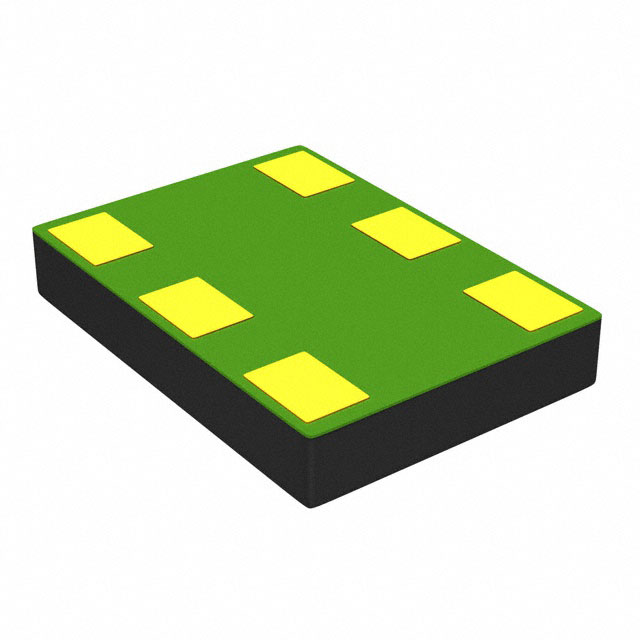
- Part No.:
- LMK61A2-644M53SIAR
- Manufacturer:
- Texas Instruments
- Category:
- Oscillators
- Package:
- 6-SMD Module
- Datasheet:
-
 LMK61A2-644M53SIAR.pdf
- Description:
- SILIC OSC XO 644.5313MHZ LVDS
- Quantity:
- Payment:

- Shipping:

Inventory:4,835
Please send an inquiry. Send us your inquiry, and we will respond immediately.
Product details
Overview
LMK61A2-644M53SIAR from Texas Instruments is an ultra-low jitter LVDS oscillator generating a precise 644.53125 MHz reference clock for high-speed serial interfaces. It delivers ±50 ppm total frequency stability, 90 fs RMS jitter (typical at >100 MHz), and operates from a single 3.3 V supply in industrial temperature range (–40°C to +85°C). Its primary role is timing reference generation in FPGA transceiver lanes and optical transport systems.
For engineers reviewing the LMK61A2-644M53SIAR datasheet, LMK61A2-644M53SIAR pinout, LMK61A2-644M53SIAR application, or LMK61A2-644M53SIAR equivalent, key selection criteria include differential output format compatibility (LVDS), 644.53125 MHz exact frequency requirement, sub-100 fs jitter performance, PSRR of –70 dBc, and 7 mm × 5 mm QFM package constraints.
Technical Context
The LMK61A2-644M53SIAR implements an integrated PLL-based architecture with factory-programmed frequency synthesis, eliminating external crystal or loop filter components. Its internal power conditioning provides robust supply noise immunity, enabling direct integration into noisy digital power domains without additional filtering.
It supports only LVDS output format at this specific frequency variant, with differential pair (OUTP/OUTN) termination optimized for 100 Ω differential loads. The OE pin enables LVCMOS-compatible output disable control with internal pull-up, allowing dynamic power gating in system-level timing management.
Key Specifications
| Parameter | Value and Actual Design Meaning |
|---|---|
| Output Frequency | 644.53125 MHz - exact frequency required for OTU4/100G Ethernet and CPRI 24.33 Gbps line rates. |
| Output Format | LVDS - differential signaling with 300–480 mV swing, compatible with FPGA I/O banks and ASIC clock inputs requiring low-noise, low-power differential clocks. |
| RMS Phase Jitter (12 kHz–20 MHz) | 150–300 fs - measured specifically at 644.53125 MHz, meeting stringent jitter budgets for 100G+ SerDes PHYs. |
| Total Frequency Tolerance | ±50 ppm - includes initial tolerance, temperature drift (–40°C to +85°C), voltage variation, solder reflow shift, and 10-year aging. |
| Supply Voltage | 3.3 V ± 5% - single-rail operation simplifies power delivery; no separate analog/digital supplies needed. |
| PSRR | –70 dBc - suppresses 50 mVpp ripple at 50 kHz–1 MHz on VDD, reducing need for ultra-low-noise LDOs. |
| Package | 6-pin QFM (7.0 mm × 5.0 mm) - industry-standard 7050 footprint, enabling drop-in replacement for legacy XOs. |
Pinout & Package
LMK61A2-644M53SIAR uses a 6-pin QFM (Quad Flat No-lead) package measuring 7.0 mm × 5.0 mm, pin-compatible with standard 7050 XO footprints. Thermal pad is connected to GND for optimal heat dissipation.
| Pin/Terminal | Circuit Role | Design Meaning |
|---|---|---|
| 1 - NC | No Connect | Unbonded die pad; must be left floating or tied to GND per layout guidelines - no electrical function. |
| 2 - OE | Output Enable Input | LVCMOS input with internal pull-up; drives outputs to high-impedance when logic low (VIL ≤ 0.6 V). |
| 3 - GND | Ground Reference | Analog/digital common ground; requires ≥3 thermal vias to internal ground plane for thermal and noise integrity. |
| 4 - OUTN | Differential Output (Negative) | LVDS-compliant negative leg; paired with OUTP to deliver 100 Ω differential signal with 300–480 mV swing. |
| 5 - OUTP | Differential Output (Positive) | LVDS-compliant positive leg; forms true differential pair with OUTN for common-mode noise rejection. |
| 6 - VDD | Power Supply | 3.3 V ± 5% analog supply; requires local 10 µF / 1 µF / 0.1 µF decoupling network with short trace routing. |
Key Features
| Feature | Design Value |
|---|---|
| Ultra-low jitter at 644.53125 MHz | 150–300 fs RMS (12 kHz–20 MHz) - meets SONET OC-192, OTU4, and 100G KR4 jitter compliance thresholds. |
| Factory-programmed fixed frequency | No external configuration required - eliminates EEPROM, programming hardware, or firmware overhead during production. |
| High PSRR (–70 dBc) | Enables direct connection to switched-mode power supply rails without dedicated low-noise LDO, reducing BOM count and board area. |
| Industrial temperature operation | Full specification guaranteed from –40°C to +85°C - suitable for base station radios, network switches, and industrial compute platforms. |
| 6-pin 7050-compatible QFM | Standardized footprint allows mechanical and layout reuse across TI's LMK61XX family and third-party XO replacements. |
Applications
| OTN Transport Systems | 100G Ethernet Switches |
|---|---|
Use Scenario: Generating the 644.53125 MHz reference for OTU4 framer and FEC blocks in optical line cards. IC Role / Device Role / Timing Role: Primary low-jitter clock source synchronizing OTN multiplexing/demultiplexing and forward error correction engines. Use Value: Enables deterministic latency and bit-error-rate compliance under temperature and supply variation due to ±50 ppm stability and sub-300 fs jitter. |
Use Scenario: Providing reference clock to QSFP28/OSFP transceivers and switch fabric ASICs in data center top-of-rack switches. IC Role / Device Role / Timing Role: System-level timing reference for 100G KR4/CR4 SerDes lanes and packet processing clock domains. Use Value: Maintains SERDES lock and BER < 1e–12 over full industrial temperature range via robust PSRR and LVDS drive strength. |
| FPGA-Based Test Equipment | CPRI Remote Radio Heads |
Use Scenario: Driving high-speed ADC/DAC sampling clocks and FPGA transceiver reference inputs in modular instrumentation platforms. IC Role / Device Role / Timing Role: Ultra-low phase noise clock generator for coherent signal generation and analysis subsystems. Use Value: Delivers –162 dBc/Hz phase noise floor at 10 MHz offset, preserving SFDR in wideband RF measurement applications. |
Use Scenario: Supplying the 644.53125 MHz clock for CPRI Option 10 (24.33 Gbps) interface between BBU and remote radio head. IC Role / Device Role / Timing Role: Synchronization source for CPRI link timing recovery and baseband IQ data alignment. Use Value: Ensures deterministic inter-RH synchronization and reduces timing skew-induced EVM degradation in massive MIMO deployments. |
Equivalent & Alternatives
The following parts are listed as comparable options for similar ultra-low jitter oscillator applications.
| Alternative Part | Technical Difference | Application Difference | Selection Advice |
|---|---|---|---|
| LMK61E2-644M53SIAR | Same 644.53125 MHz LVDS output, but ±25 ppm total frequency tolerance (LMK61X0 grade vs. LMK61X2 grade). | Targeted for telecom infrastructure requiring tighter long-term stability; higher cost and longer lead time. | Select when aging and temperature drift budget is < ±25 ppm over 10 years; otherwise LMK61A2-644M53SIAR suffices for industrial-grade systems. |
| Si5338A-D-GM | Programmable I2C-based clock generator; supports 644.53125 MHz but requires external configuration; 125 fs RMS jitter (typical). | Used where multi-frequency flexibility or spread-spectrum capability is needed; larger 4×4 mm QFN package. | Choose only if programmability justifies added complexity; LMK61A2-644M53SIAR offers lower risk, faster time-to-market for fixed-frequency use. |
Compared with LMK61E2-644M53SIAR, the LMK61A2-644M53SIAR trades ±25 ppm stability for broader industrial qualification and lower cost; versus Si5338A-D-GM, it eliminates I²C dependency and reduces layout complexity while maintaining sufficient jitter performance for 100G applications.
Availability
LMK61A2-644M53SIAR is available at Aetrix Electronics and suitable for OTN transport systems, 100G Ethernet switches, and FPGA-based test equipment requiring stable component supply, consistent parametric performance, and long-term lifecycle support.
Supply support for LMK61A2-644M53SIAR includes scheduled delivery planning, volume procurement assistance, BOM continuity management, traceable sourcing, and lifecycle availability coordination for OEM customers, industrial embedded developers, connected-device designers, and electronics production programs.
Manufacturer
Texas Instruments is a global semiconductor company specializing in analog, embedded processing, and high-performance timing solutions, with decades of leadership in precision clock generation.
The LMK61XX product line was designed specifically for high-speed communication infrastructure, delivering factory-programmed, ultra-low jitter oscillators that replace quartz-based solutions in 10G–400G networking, optical transport, and wireless baseband applications.
FAQ
What output format does the LMK61A2-644M53SIAR support?
The LMK61A2-644M53SIAR supports LVDS output only at its factory-programmed frequency of 644.53125 MHz. Unlike other variants in the LMK61XX family, this part is not configurable for LVPECL or HCSL. Its LVDS output delivers 300–480 mV differential swing into 100 Ω loads, with guaranteed rise/fall times of 150–250 ps.
Does the LMK61A2-644M53SIAR require external programming or configuration?
No, the LMK61A2-644M53SIAR is factory-programmed and fully operational upon power-up with no external configuration required. It contains no EEPROM or I²C interface. All timing parameters-including frequency, output format, and startup behavior-are hard-coded during manufacturing, ensuring zero firmware dependencies and deterministic boot timing for the LMK61A2-644M53SIAR.
What is the recommended power supply bypassing for the LMK61A2-644M53SIAR?
Texas Instruments specifies a three-capacitor bypass network for the LMK61A2-644M53SIAR: 10 µF (bulk), 1 µF (mid-frequency), and 0.1 µF (high-frequency) ceramic capacitors placed as close as possible to the VDD pin. All capacitors must be mounted on the component side using 0201 or 0402 packages, with short traces and low-inductance connections to the ground plane via multiple vias.
How does the OE pin function on the LMK61A2-644M53SIAR?
The OE (Output Enable) pin on the LMK61A2-644M53SIAR is an LVCMOS input with internal pull-up. When pulled low (≤0.6 V), it disables both OUTP and OUTN outputs, placing them in high-impedance state within 50 µs. When left unconnected or pulled high (≥1.4 V), outputs are active. This enables system-level clock gating without affecting internal oscillator operation.
Is the LMK61A2-644M53SIAR pin-compatible with other LMK61XX devices?
Yes, the LMK61A2-644M53SIAR shares identical 6-pin QFM (7.0 mm × 5.0 mm) packaging and pinout with all members of the LMK61XX family, including LMK61E2-100M, LMK61A2-125M, and LMK61I2-100M. Pin functions (OE, GND, OUTN, OUTP, VDD, NC) are consistent across variants, enabling PCB design reuse and simplified inventory management for the LMK61A2-644M53SIAR and related parts.
LMK61A2-644M53SIAR Specifications
- Product attributes
- Attribute value
- Manufacturer:
- Texas Instruments
- Series:
- LMK61XX
- Package/Case:
- 6-SMD Module
- Packaging:
- Tape & Reel (TR)
- Product Status:
- Active
- Base Resonator:
- Silicon
- Type:
- XO (Standard)
- Frequency:
- 644.53125 MHz
- Function:
- Enable/Disable
- Output:
- LVDS
- Voltage - Supply:
- 3.3V
- Frequency Stability:
- ±50ppm
- Absolute Pull Range (APR):
- -
- Operating Temperature:
- -40°C ~ 85°C
- Spread Spectrum Bandwidth:
- -
- Current - Supply (Max):
- 196mA
- Ratings:
- -
- Mounting Type:
- Surface Mount
- Supplier Device Package:
- 6-QFM (7x5)
- Size / Dimension:
- 0.276" L x 0.197" W (7.00mm x 5.00mm)
- Height - Seated (Max):
- 0.045" (1.15mm)
LMK61A2-644M53SIAR FAQ
1.How can I place an order for LMK61A2-644M53SIAR through Aetrix?
Please submit a Request for Quotation (RFQ) for LMK61A2-644M53SIAR on Aetrix. Our sales agent will provide a competitive quotation and guide you through the order confirmation once you accept the terms.
2.Are the price and stock information for LMK61A2-644M53SIAR reliable?
The price and inventory of LMK61A2-644M53SIAR are updated periodically and may fluctuate due to market conditions. Stock and pricing data are typically refreshed every 24 hours. Quotation validity for LMK61A2-644M53SIAR is usually 5 days.
3.What payment methods are accepted for LMK61A2-644M53SIAR?
We accept Wire Transfer, PayPal, Credit Card, Western Union, MoneyGram, and Escrow for LMK61A2-644M53SIAR transactions.
Note: Certain payment methods may incur a processing fee.
4.How is shipping managed for LMK61A2-644M53SIAR?
LMK61A2-644M53SIAR orders can be shipped via leading logistics carriers, including DHL, UPS, FedEx, TNT, or Registered Mail.
Once your LMK61A2-644M53SIAR order is processed, you will receive an email with the shipment details and tracking number.
Note: Tracking information may take up to 24 hours to appear. Express delivery typically takes 3–5 business days.
5.How can I obtain technical support or documentation for LMK61A2-644M53SIAR?
For technical support, including LMK61A2-644M53SIAR datasheets, pinout diagrams, or application guidance, please contact our engineering support team. They can provide detailed documentation and assistance for your LMK61A2-644M53SIAR requirements.
6.How does Aetrix verify that LMK61A2-644M53SIAR is sourced from the original manufacturer or authorized distributors?
All LMK61A2-644M53SIAR products on Aetrix are procured from qualified distributors and authorized channels. Our dedicated quality assurance team conducts strict verification, including traceability checks and, if necessary, third-party testing. This ensures that LMK61A2-644M53SIAR meets industry standards.
7.What is the process for return or replacement of LMK61A2-644M53SIAR?
All LMK61A2-644M53SIAR units undergo pre-shipment inspection (PSI). If there is an issue with LMK61A2-644M53SIAR, returns or replacements are accepted under the following conditions:
1.Quantity discrepancies, incorrect items, or visible external defects (such as breakage or corrosion), acknowledged by Aetrix.
2.The issue is reported within 90 days of delivery.
3.The LMK61A2-644M53SIAR part is unused and in its original packaging.
Return procedure for LMK61A2-644M53SIAR:
1.Submit a request within 90 days.
2.Obtain a Return Material Authorization (RMA) from Aetrix.
LMK61A2-644M53SIAR Tags
-
ECS-2333-160-BN-TR
ECS Inc.
-
ECS-2333-240-BN-TR
ECS Inc.
-
KC2016Z25.0000C1KX00
KYOCERA AVX
-0.035-Thick.jpg)
-
ECS-2033-250-BN
ECS Inc.
-
O 25,0-JO32-B-1V3-1-T1-LF
Jauch Quartz
-
SIT1533AI-H4-DCC-32.768E
SiTime
-
ECS-2333-500-BN-TR
ECS Inc.
-
COM1305-50.000-EXT-T-TR
Raltron Electronics
-
SG-210STF 24.0000ML0
EPSON
-
ECS-3225MV-320-CN-TR
ECS Inc.
-
ECS-2033-240-BN
ECS Inc.
-
ECS-2333-120-BN-TR
ECS Inc.
Tech Hub

A practical engineering guide to 3.3V and 5V logic compatibility, input thresholds, resistor dividers, translator ICs, MOSFET level shifting, I2C pull-ups, timing limits and power-sequencing risks.

The 74HC595 uses push-pull logic outputs, while the TPIC6B595 uses 50 V open-drain DMOS sinks for higher-power loads. This guide compares timing, current limits, 3.3 V interfacing, load wiring, thermal…

The 74HC595 converts serial data into eight stable parallel outputs. This guide covers pin functions, shift and storage timing, OE and MR behavior, drive-current limits, cascading, voltage compatibilit…

A technical comparison of level-sensitive latches and edge-triggered flip-flops, covering timing windows, setup and hold limits, master–slave operation, time borrowing, race-through, HDL inference and…

A D latch stores one bit while Enable controls when data can pass. This reference covers gate-level operation, truth tables, transparency, setup and hold timing, LE versus OE, common ICs and practical …

An SR latch stores one bit through cross-coupled feedback. This engineering reference covers NOR and NAND implementations, truth tables, forbidden-state recovery, gated operation, switch debouncing, fa…

Latch circuits retain one bit through feedback. This technical reference covers SR and D latches, truth tables, transparency, timing limits, latch-versus-flip-flop behavior, applications and common log…

An engineering guide to LED driver operation, constant-current and constant-voltage outputs, linear and switching topologies, dimming, IC selection, calculations, replacement compatibility, and fault c…

Operational amplifier guide covering op amp basics, feedback, ideal vs real op amps, common configurations, buffer circuits, offset, bias current, gain-bandwidth, slew rate, rail-to-rail limits and sel…

Jumper cables guide covering safe connection order, red and black clamp placement, final ground connection, cable gauge, length, clamp quality, copper vs CCA cables, jump starter comparison and battery…


