
 My Inquiry
 My Account


Texas Instruments LMK62I0-156M25SIAT
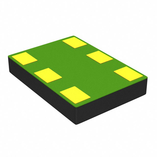
- Part No.:
- LMK62I0-156M25SIAT
- Manufacturer:
- Texas Instruments
- Category:
- Oscillators
- Package:
- 6-SMD Module
- Datasheet:
-
 LMK62I0-156M25SIAT.pdf
- Description:
- SILICONE OSC XO 156.2500MHZ HCSL
- Quantity:
- Payment:

- Shipping:

Inventory:382
Please send an inquiry. Send us your inquiry, and we will respond immediately.
Product details
Overview
LMK62I0-156M25SIAT from Texas Instruments is a factory-programmed, low-jitter HCSL oscillator delivering 156.25 MHz output with ±25 ppm total frequency stability, 3.3-V supply operation, and 150 fs RMS phase jitter (12 kHz–20 MHz) over –40°C to +85°C. It serves as a high-stability timing reference for FPGA clocking, Base Band Unit (BBU) synchronization, and high-speed serial interface recovery in telecom infrastructure.
For engineers reviewing the LMK62I0-156M25SIAT datasheet, LMK62I0-156M25SIAT pinout, LMK62I0-156M25SIAT application, or LMK62I0-156M25SIAT equivalent, this device is selected for its HCSL drive capability, robust PSRR (–60 dBc), industrial temperature range, and pin-compatible 5-mm × 3.2-mm QFM package-critical for space-constrained, noise-sensitive clock distribution networks.
Technical Context
The LMK62I0-156M25SIAT integrates a high-performance PLL-based oscillator core with internal power conditioning to suppress supply noise, enabling stable 156.25 MHz HCSL output without external loop filters. Its differential HCSL output complies with JEDEC HCSL v1.0 specifications, featuring VOH ≥ 660 mV, VOL ≤ 100 mV, and VCROSS between 250–475 mV.
Operation requires only a single 3.3-V ±5% supply and supports output enable control via LVCMOS OE input (VIH = 1.4 V, VIL = 0.6 V), with 50 µs enable/disable timing and internal pulldown. Startup completes within 10 ms after VDD reaches 3.135 V.
Key Specifications
| Parameter | Value and Actual Design Meaning |
|---|---|
| Output Frequency | 156.25 MHz - precisely matched to Ethernet, CPRI, and PCIe Gen1/2 reference clock requirements. |
| Output Format | HCSL - provides 50-Ω source-terminated differential signaling compatible with FPGA and ASIC clock inputs without external resistors. |
| Frequency Stability | ±25 ppm - includes initial tolerance, temperature drift (–40°C to +85°C), voltage variation, solder reflow shift, and 5-year aging at 40°C. |
| Phase Jitter (RMS) | 150 fs (typ.) - measured 12 kHz–20 MHz; enables <0.1 UI jitter budget in 10G+ serial links. |
| PSRR | –60 dBc - rejects 50-mVpp ripple at 50 kHz–1 MHz on VDD, reducing need for ultra-low-noise LDOs. |
| Supply Voltage | 3.3 V ±5% - operates from standard system rail; consumes 90–105 mA (HCSL mode). |
| Package | 6-pin QFM (SIA), 5.0 mm × 3.2 mm - industry-standard 5032 footprint for drop-in replacement of legacy XOs. |
Pinout & Package
The LMK62I0-156M25SIAT uses a 6-pin Quad Flat Module (QFM) package designated SIA, measuring 5.0 mm × 3.2 mm with 1.1 mm max height and pin-compatible footprint with industry-standard 5032 crystal oscillators.
| Pin/Terminal | Circuit Role | Design Meaning |
|---|---|---|
| 1 (OE) | Digital control input | LVCMOS output enable with internal pulldown; pull up externally with 10 kΩ to enable output; 50 µs response time. |
| 2 (NC) | No-connect | Unbonded pad; must be left floating or grounded per layout best practice-no electrical function. |
| 3 (GND) | Power ground | Primary analog/digital return; requires ≥3 thermal vias to inner ground plane for thermal and EMI performance. |
| 4 (OUTP) | Differential output (+) | HCSL high-side output; 50-Ω source impedance; pairs with OUTN for true differential signaling. |
| 5 (OUTN) | Differential output (–) | HCSL low-side output; complements OUTP; crossing point (VCROSS) controlled to 250–475 mV. |
| 6 (VDD) | Analog power supply | 3.3-V ±5% input; requires local 10 µF / 1 µF / 0.1 µF decoupling; sensitive to PSRR performance. |
Key Features
| Feature | Design Value |
|---|---|
| Ultra-low phase jitter | 150 fs RMS (12 kHz–20 MHz) enables compliance with stringent SerDes jitter budgets for 10G/25G interfaces. |
| Integrated power conditioning | –60 dBc PSRR eliminates need for dedicated low-noise LDOs, simplifying power delivery network design. |
| HCSL output compliance | Meets JEDEC HCSL v1.0: VOH ≥ 660 mV, VOL ≤ 100 mV, dV/dt = 1–3 V/ns, ODC = 45–55%. |
| Industrial temperature range | –40°C to +85°C ambient operation with guaranteed 105°C junction limit ensures reliability in telecom and embedded systems. |
| Precision frequency stability | ±25 ppm total tolerance covers aging, temp, voltage, and reflow-reducing need for field calibration. |
Applications
| 10G/25G Ethernet Switching | FPGA High-Speed Clocking |
|---|---|
Use Scenario: Reference clock for 10GBASE-R/25GBASE-R PHYs and switch fabric ASICs in data center top-of-rack switches. IC Role / Device Role / Timing Role: Primary low-jitter clock source driving serializer/deserializer (SerDes) PLLs and MAC timing blocks. Use Value: 150 fs jitter and ±25 ppm stability ensure bit error rate (BER) <1e–12 under worst-case channel loss and crosstalk. | Use Scenario: System clock input for Xilinx Versal or Intel Agilex FPGAs in high-throughput compute acceleration platforms. IC Role / Device Role / Timing Role: Dedicated HCSL reference for transceiver banks and hardened processor subsystems. Use Value: Pin-compatible 5032 footprint and HCSL drive eliminate external termination, saving PCB area and signal integrity risk. |
| 5G Base Band Unit (BBU) | Medical Imaging Data Acquisition |
Use Scenario: Synchronization clock for CPRI/eCPRI fronthaul interfaces between radio units and centralized BBU in 5G NR deployments. IC Role / Device Role / Timing Role: Stratum-3-equivalent timing reference meeting ITU-T G.8262 EEC-2 wander requirements. Use Value: –60 dBc PSRR maintains timing accuracy despite noisy baseband power rails shared with RF front-end ICs. | Use Scenario: Sampling clock for multi-channel ADCs in MRI and CT scanner front-end modules requiring deterministic latency. IC Role / Device Role / Timing Role: Low-phase-noise master clock for time-interleaved ADC arrays and digital beamforming engines. Use Value: 150 fs jitter directly translates to <0.05 LSB noise floor degradation in 16-bit, 125 MSPS ADC systems. |
Equivalent & Alternatives
The following parts are listed as comparable options for similar oscillator applications.
| Alternative Part | Technical Difference | Application Difference | Selection Advice |
|---|---|---|---|
| LMK62A2-156M25SIAT | LVDS output instead of HCSL; same 156.25 MHz, ±25 ppm, and package. | Requires external 100-Ω differential termination; lower drive strength than HCSL. | Select when interfacing with LVDS-input FPGAs or ASICs where common-mode voltage (1.125–1.375 V) is preferred. |
| LMK62E0-156M25SIAT | LVPECL output; higher power (110 mA vs. 105 mA); same frequency and stability. | Needs negative termination (150 Ω to VCC–2 V); incompatible with HCSL/LVDS receivers without level-shifting. | Choose for legacy systems using LVPECL clock trees or where higher output swing (700–1200 mV) is required. |
Compared with LMK62A2-156M25SIAT and LMK62E0-156M25SIAT, the LMK62I0-156M25SIAT offers optimal integration for modern FPGAs with native HCSL inputs-eliminating termination components, reducing power vs. LVPECL, and providing better noise immunity than LVDS in dense PCB layouts.
Availability
LMK62I0-156M25SIAT is available at Aetrix Electronics and suitable for 5G infrastructure, high-performance computing, and medical imaging systems requiring stable component supply, long-term lifecycle support, and traceable sourcing.
Supply support for LMK62I0-156M25SIAT includes scheduled delivery planning, volume procurement assistance, BOM continuity management, traceable sourcing, and lifecycle availability coordination for OEM customers, industrial embedded developers, connected-device designers, and electronics production programs.
Manufacturer
Texas Instruments is a global semiconductor leader specializing in analog, embedded processing, and clock solutions, with decades of expertise in precision timing and signal integrity.
The LMK62XX family is designed for high-speed digital systems demanding ultra-low jitter, excellent PSRR, and flexible output formats-targeting telecom, datacenter, test equipment, and industrial FPGA-based platforms.
FAQ
What is the recommended power supply bypassing scheme for LMK62I0-156M25SIAT?
TI specifies a three-capacitor network: 10 µF (bulk), 1 µF (mid-frequency), and 0.1 µF (high-frequency), all placed as close as possible to the VDD pin with short, low-inductance traces to GND. Use 0201 or 0402 case sizes, mount on the component side, and connect GND via ≥3 thermal vias to minimize impedance and maximize PSRR effectiveness.
Can LMK62I0-156M25SIAT be used with LVDS or LVPECL receivers?
No-LMK62I0-156M25SIAT is factory-configured exclusively for HCSL output. Its VOH/VOL levels (660–900 mV / –100–100 mV) and 50-Ω source termination do not meet LVDS (300–480 mV swing, 107-Ω Z₀) or LVPECL (700–1200 mV, 150-Ω termination) specifications. Interfacing requires an external level translator or selection of LMK62A2- or LMK62E0-series variants.
What is the function of the NC pin (Pin 2) on LMK62I0-156M25SIAT?
Pin 2 is a no-connect (NC) terminal with no internal bond wire or circuit connection. TI's datasheet explicitly defines it as "N/A" and recommends leaving it unconnected-neither grounded nor tied to any voltage. Routing copper under this pad is acceptable, but no signal or power should be assigned to it.
How does the OE pin behave during power-up if left unconnected?
The OE pin has an internal pulldown resistor, so if left unconnected (floating), it defaults to logic low-disabling the output pair and placing OUTP/OUTN in high-impedance state. To enable output, OE must be actively driven high (≥1.4 V) via external 10 kΩ pullup or controller GPIO; startup delay from OE assertion to valid output is 50 µs.
LMK62I0-156M25SIAT Specifications
- Product attributes
- Attribute value
- Manufacturer:
- Texas Instruments
- Series:
- LMK62XX
- Package/Case:
- 6-SMD Module
- Packaging:
- Tape & Reel (TR)
- Product Status:
- Not For New Designs
- Base Resonator:
- Silicon
- Type:
- XO (Standard)
- Frequency:
- 156.25 MHz
- Function:
- Enable/Disable
- Output:
- HCSL
- Voltage - Supply:
- 3.3V
- Frequency Stability:
- ±25ppm
- Absolute Pull Range (APR):
- -
- Operating Temperature:
- -40°C ~ 85°C
- Spread Spectrum Bandwidth:
- -
- Current - Supply (Max):
- 105mA
- Ratings:
- -
- Mounting Type:
- Surface Mount
- Supplier Device Package:
- 6-QFM (7x5)
- Size / Dimension:
- 0.197" L x 0.126" W (5.00mm x 3.20mm)
- Height - Seated (Max):
- 0.043" (1.10mm)
LMK62I0-156M25SIAT FAQ
1.How can I place an order for LMK62I0-156M25SIAT through Aetrix?
Please submit a Request for Quotation (RFQ) for LMK62I0-156M25SIAT on Aetrix. Our sales agent will provide a competitive quotation and guide you through the order confirmation once you accept the terms.
2.Are the price and stock information for LMK62I0-156M25SIAT reliable?
The price and inventory of LMK62I0-156M25SIAT are updated periodically and may fluctuate due to market conditions. Stock and pricing data are typically refreshed every 24 hours. Quotation validity for LMK62I0-156M25SIAT is usually 5 days.
3.What payment methods are accepted for LMK62I0-156M25SIAT?
We accept Wire Transfer, PayPal, Credit Card, Western Union, MoneyGram, and Escrow for LMK62I0-156M25SIAT transactions.
Note: Certain payment methods may incur a processing fee.
4.How is shipping managed for LMK62I0-156M25SIAT?
LMK62I0-156M25SIAT orders can be shipped via leading logistics carriers, including DHL, UPS, FedEx, TNT, or Registered Mail.
Once your LMK62I0-156M25SIAT order is processed, you will receive an email with the shipment details and tracking number.
Note: Tracking information may take up to 24 hours to appear. Express delivery typically takes 3–5 business days.
5.How can I obtain technical support or documentation for LMK62I0-156M25SIAT?
For technical support, including LMK62I0-156M25SIAT datasheets, pinout diagrams, or application guidance, please contact our engineering support team. They can provide detailed documentation and assistance for your LMK62I0-156M25SIAT requirements.
6.How does Aetrix verify that LMK62I0-156M25SIAT is sourced from the original manufacturer or authorized distributors?
All LMK62I0-156M25SIAT products on Aetrix are procured from qualified distributors and authorized channels. Our dedicated quality assurance team conducts strict verification, including traceability checks and, if necessary, third-party testing. This ensures that LMK62I0-156M25SIAT meets industry standards.
7.What is the process for return or replacement of LMK62I0-156M25SIAT?
All LMK62I0-156M25SIAT units undergo pre-shipment inspection (PSI). If there is an issue with LMK62I0-156M25SIAT, returns or replacements are accepted under the following conditions:
1.Quantity discrepancies, incorrect items, or visible external defects (such as breakage or corrosion), acknowledged by Aetrix.
2.The issue is reported within 90 days of delivery.
3.The LMK62I0-156M25SIAT part is unused and in its original packaging.
Return procedure for LMK62I0-156M25SIAT:
1.Submit a request within 90 days.
2.Obtain a Return Material Authorization (RMA) from Aetrix.
LMK62I0-156M25SIAT Tags
-
ECS-2333-160-BN-TR
ECS Inc.
-
ECS-2333-240-BN-TR
ECS Inc.
-
KC2016Z25.0000C1KX00
KYOCERA AVX
-0.035-Thick.jpg)
-
ECS-2033-250-BN
ECS Inc.
-
O 25,0-JO32-B-1V3-1-T1-LF
Jauch Quartz
-
SIT1533AI-H4-DCC-32.768E
SiTime
-
ECS-2333-500-BN-TR
ECS Inc.
-
COM1305-50.000-EXT-T-TR
Raltron Electronics
-
SG-210STF 24.0000ML0
EPSON
-
ECS-3225MV-320-CN-TR
ECS Inc.
-
ECS-2033-240-BN
ECS Inc.
-
ECS-2333-120-BN-TR
ECS Inc.
Tech Hub

Jumper cables guide covering safe connection order, red and black clamp placement, final ground connection, cable gauge, length, clamp quality, copper vs CCA cables, jump starter comparison and battery…

LDO regulator guide covering low dropout voltage, power dissipation, thermal design, PSRR, output noise, capacitor stability, adjustable LDO circuits, LDO vs buck converter and datasheet selection chec…

Conditional Access Module guide covering CAM meaning, CI/CI+ interface, smart card authorization, DVB security workflow, TV and set-top box compatibility, internal electronics, ESD protection, connecto…

Guide to electronic component obsolescence covering EOL risk, PCN/PDN notices, last-time buy planning, replacement options, form-fit-function validation, counterfeit risk and BOM lifecycle management.

18650 battery guide covering lithium-ion cell basics, 3.6V/3.7V voltage, 4.2V charging, mAh and Wh capacity, protected cells, chargers, BMS, series-parallel packs, holders, welding and sourcing checks.…

Hall effect sensor guide covering working principle, linear and digital sensors, Arduino circuits, current sensing, speed detection, automotive applications, A3144 examples, signal filtering and datash…

Product Change Notification guide for electronic components, covering PCN meaning, PCN vs PDN/EOL, common change types, risk levels, form-fit-function review, engineering validation, BOM control, LTB/L…

A practical guide to blend door actuators, covering HVAC function, symptoms, location, AC and heater issues, reset and calibration, replacement cost, electrical diagnosis, compatibility checks, and rep…

Engineering guide to Raspberry Pi alternatives, covering chip-level differences, Orange Pi, ROCK, Jetson, Banana Pi, NanoPi, Compute Module, Pico, GPIO, camera, HAT compatibility, and replacement risks…

Engineering guide to dynamic load response testing for high-current buck converters, covering load step setup, slew rate, Vcore undershoot, overshoot, recovery time, probe location, output capacitors a…


